In this chapter we examine how the concepts in Chapter 4 can be used to build some of the logic circuits that make up a CPU, Memory, and other devices. We will not describe an entire unit, only a few small parts. The goal is to provide an introductory overview of the concepts. There are many excellent books that cover the details. For example, see [20], [23], or [24] for circuit design details and [28], [31], [34] for CPU architecture design concepts.
Logic circuits can be classified as either
An example of the two concepts is a television remote control. You can enter a number and the output (a particular television channel) depends only on the number entered. It does not matter what channels been viewed previously. So the relationship between the input (a number) and the output is combinational.
The remote control also has inputs for stepping either up or down one channel. When using this input method, the channel selected depends on what channel has been previously selected and the sequence of up/down button pushes. The channel up/down buttons illustrate a sequential input/output relationship.
Although a more formal definition will be given in Section 5.3, this television example also illustrates the concept of state. My television remote control has a button I can push that will show the current channel setting. If I make a note of the beginning channel setting, and keep track of the sequence of channel up and down button pushes, I will know the ending channel setting. It does not matter how I originally got to the beginning channel setting. The channel setting is the state of the channel selection mechanism because it tells me everything I need to know in order to select a new channel by using a sequence of channel up and down button pushes.
Combinational logic circuits have no memory. The output at any given time depends completely upon the circuit configuration and the input(s).
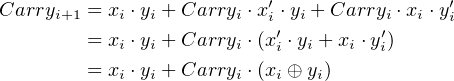
One of the most fundamental operations the ALU must do is to add two bits. We begin with two definitions. (The reason for the names will become clear later in this section.)
xi | yi | Carryi+1 | Sumi |
0 | 0 | 0 | 0 |
0 | 1 | 0 | 1 |
1 | 0 | 0 | 1 |
1 | 1 | 1 | 0 |
where xi is the ith bit of the multiple bit value, x; y i is the ith bit of the multiple bit value, y; Sum i is the ith bit of the multiple bit value, Sum; Carry i+1 is the carry from adding the next-lower significant bits, xi, yi.
Carryi | xi | yi | Carryi+1 | Sumi |
0 | 0 | 0 | 0 | 0 |
0 | 0 | 1 | 0 | 1 |
0 | 1 | 0 | 0 | 1 |
0 | 1 | 1 | 1 | 0 |
1 | 0 | 0 | 0 | 1 |
1 | 0 | 1 | 1 | 0 |
1 | 1 | 0 | 1 | 0 |
1 | 1 | 1 | 1 | 1 |
where xi is the ith bit of the multiple bit value, x; y i is the ith bit of the multiple bit value, y; Sum i is the ith bit of the multiple bit value, Sum; Carry i+1 is the carry from adding the next-lower significant bits, xi, yi, and Carryi.
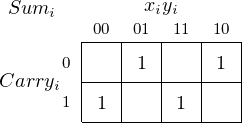
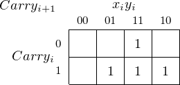
First, let us look at the Karnaugh map for the sum:
There are no obvious groupings. We can write the function as a sum of product terms from the Karnaugh map.
 | (5.1) |
In the Karnaugh map for carry:
we can see three groupings:
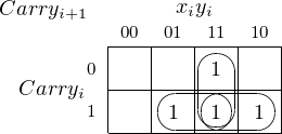
These groupings yield a three-term function that defines when Carryi+1 = 1:
 | (5.2) |
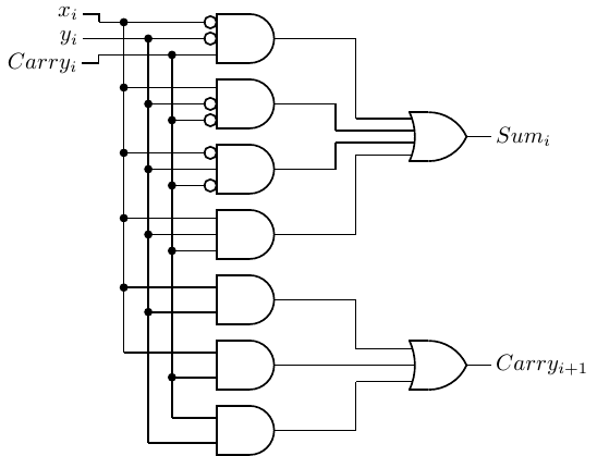
Equations 5.1 and 5.2 lead directly to the circuit for an adder in Figure 5.1.
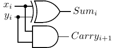
For a different approach, we look at the definition of half adder. The sum is simply the XOR of the two inputs, and the carry is the AND of the two inputs. This leads to the circuit in Figure 5.2.
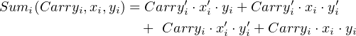
Instead of using Karnaugh maps, we will perform some algebraic manipulations on Equation 5.1. Using the distribution rule, we can rearrange:
 | (5.3) |
Let us manipulate the last product term in Equation 5.3.
 |
Thus,
 | (5.4) |
Similarly, we can rewrite Equation 5.2:
 | (5.5) |
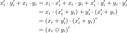
You should be able to see two other possible groupings on this Karnaugh map and may wonder why they are not circled here. The two ungrouped minterms, Carryi ⋅ xi′⋅ yi and Carryi ⋅ xi ⋅ yi′, form a pattern that suggests an exclusive or operation.
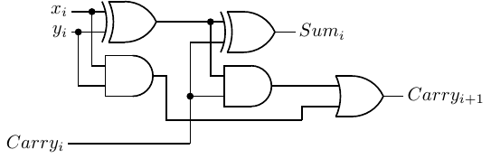
Notice that the first product term in Equation 5.5, xi ⋅ yi, is generated by the Carry portion of a half-adder, and that the exclusive or portion, xi ⊕yi, of the second product term is generated by the Sum portion. A logic gate implementation of a full adder is shown in Figure 5.3.
You can see that it is implemented using two half adders and an OR gate. And now you understand the terminology “half adder” and “full adder.”
We cannot say which of the two adder circuits, Figure 5.1 or Figure 5.3, is better from just looking at the logic circuits. Good engineering design depends on many factors, such as how each logic gate is implemented, the cost of the logic gates and their availability, etc. The two designs are given here to show that different approaches can lead to different, but functionally equivalent, designs.
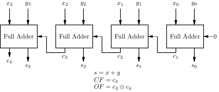
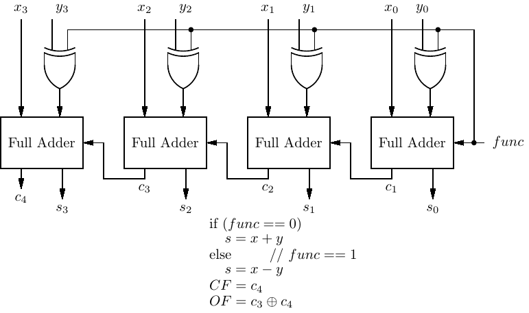
An n-bit adder can be implemented with n full adders. Figure 5.4 shows a 4-bit adder.
Addition begins with the full adder on the right receiving the two lowest-order bits, x0 and y0. Since this is the lowest-order bit there is no carry and c0 = 0. The bit sum is s0, and the carry from this addition, c1, is connected to the carry input of the next full adder to the left, where it is added to x1 and y1.
So the ith full adder adds the two ith bits of the operands, plus the carry (which is either 0 or 1) from the (i − 1)th full adder. Thus, each full adder handles one bit (often referred to as a “slice”) of the total width of the values being added, and the carry “ripples” from the lowest-order place to the highest-order.
The final carry from the highest-order full adder, c4 in the 4-bit adder of Figure 5.4, is stored in the CF bit of the Flags register (see Section 6.2). And the exclusive or of the final carry and penultimate carry, c4 ⊕ c3 in the 4-bit adder of Figure 5.4, is stored in the OF bit.
Recall that in the 2’s complement code for storing integers a number is negated by taking its 2’s complement. So we can subtract y from x by doing:
![x − y = x + (2’s complement of y)
= x + [(y’s bits flipped)+ 1]](book162x.png) | (5.6) |
Thus, subtraction can be performed with our adder in Figure 5.4 if we complement each yi and set the initial carry in to 1 instead of 0. Each yi can be complemented by XOR-ing it with 1. This leads to the 4-bit circuit in Figure 5.5 that will add two 4-bit numbers when func = 0 and subtract them when func = 1.
There is, of course, a time delay as the sum is computed from right to left. The computation time can be significantly reduced through more complex circuit designs that pre-compute the carry.
Each instruction must be decoded by the CPU before the instruction can be carried out. In the x86-64 architecture the instruction for copying the 64 bits of one register to another register is
0100 0s0d 1000 1001 11ss sddd
where “ssss” specifies the source register and “dddd” specifies the destination register. (Yes, the bits that specify the registers are distributed through the instruction in this manner. You will learn more about this seemingly odd coding pattern in Chapter 9.) For example,
0100 0001 1000 1001 1100 0101
causes the ALU to copy the 64-bit value in register 0000 to register 1101. You will see in Chapter 9 that this instruction is written in assembly language as:
The Control Unit must select the correct two registers based on these two 4-bit patterns in the instruction. It uses a decoder circuit to perform this selection.
A decoder can be thought of as converting an n-bit input to a 2n output. But while the input can be an arbitrary bit pattern, each corresponding output value has only one bit set to 1.
In some applications not all the 2n outputs are used. For example, Table 5.1 is a truth table that shows how a decoder can be used to convert a BCD value to its corresponding decimal numeral display.
input | display
| ||||||||||||
x3 | x2 | x1 | x0 | ′9′ | ′8′ | ′7′ | ′6′ | ′5′ | ′4′ | ′3′ | ′2′ | ′1′ | ′0′ |
0 | 0 | 0 | 0 | 0 | 0 | 0 | 0 | 0 | 0 | 0 | 0 | 0 | 1 |
0 | 0 | 0 | 1 | 0 | 0 | 0 | 0 | 0 | 0 | 0 | 0 | 1 | 0 |
0 | 0 | 1 | 0 | 0 | 0 | 0 | 0 | 0 | 0 | 0 | 1 | 0 | 0 |
0 | 0 | 1 | 1 | 0 | 0 | 0 | 0 | 0 | 0 | 1 | 0 | 0 | 0 |
0 | 1 | 0 | 0 | 0 | 0 | 0 | 0 | 0 | 1 | 0 | 0 | 0 | 0 |
0 | 1 | 0 | 1 | 0 | 0 | 0 | 0 | 1 | 0 | 0 | 0 | 0 | 0 |
0 | 1 | 1 | 0 | 0 | 0 | 0 | 1 | 0 | 0 | 0 | 0 | 0 | 0 |
0 | 1 | 1 | 1 | 0 | 0 | 1 | 0 | 0 | 0 | 0 | 0 | 0 | 0 |
1 | 0 | 0 | 0 | 0 | 1 | 0 | 0 | 0 | 0 | 0 | 0 | 0 | 0 |
1 | 0 | 0 | 1 | 1 | 0 | 0 | 0 | 0 | 0 | 0 | 0 | 0 | 0 |
A 1 in a “display” column means that is the numeral that is selected by the corresponding 4-bit input value. There are six other possible outputs corresponding to the input values 1010 – 1111. But these input values are illegal in BCD, so these outputs are simply ignored.
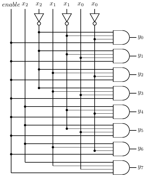
It is common for decoders to have an additional input that is used to enable the output. The truth table in Table 5.2 shows a decoder with a 3-bit input, an enable line, and an 8-bit (23) output.
enable | x2 | x1 | x0 | y7 | y6 | y5 | y4 | y3 | y2 | y1 | y0 |
0 | 0 | 0 | 0 | 0 | 0 | 0 | 0 | 0 | 0 | 0 | 0 |
0 | 0 | 0 | 1 | 0 | 0 | 0 | 0 | 0 | 0 | 0 | 0 |
0 | 0 | 1 | 0 | 0 | 0 | 0 | 0 | 0 | 0 | 0 | 0 |
0 | 0 | 1 | 1 | 0 | 0 | 0 | 0 | 0 | 0 | 0 | 0 |
0 | 1 | 0 | 0 | 0 | 0 | 0 | 0 | 0 | 0 | 0 | 0 |
0 | 1 | 0 | 1 | 0 | 0 | 0 | 0 | 0 | 0 | 0 | 0 |
0 | 1 | 1 | 0 | 0 | 0 | 0 | 0 | 0 | 0 | 0 | 0 |
0 | 1 | 1 | 1 | 0 | 0 | 0 | 0 | 0 | 0 | 0 | 0 |
1 | 0 | 0 | 0 | 0 | 0 | 0 | 0 | 0 | 0 | 0 | 1 |
1 | 0 | 0 | 1 | 0 | 0 | 0 | 0 | 0 | 0 | 1 | 0 |
1 | 0 | 1 | 0 | 0 | 0 | 0 | 0 | 0 | 1 | 0 | 0 |
1 | 0 | 1 | 1 | 0 | 0 | 0 | 0 | 1 | 0 | 0 | 0 |
1 | 1 | 0 | 0 | 0 | 0 | 0 | 1 | 0 | 0 | 0 | 0 |
1 | 1 | 0 | 1 | 0 | 0 | 1 | 0 | 0 | 0 | 0 | 0 |
1 | 1 | 1 | 0 | 0 | 1 | 0 | 0 | 0 | 0 | 0 | 0 |
1 | 1 | 1 | 1 | 1 | 0 | 0 | 0 | 0 | 0 | 0 | 0 |
The output is 0 whenever enable = 0. When enable = 1, the ith output bit is 1 if and only if the binary value of the input is equal to i. For example, when enable = 1 and x = 0112, y = 000010002. That is,
 | (5.7) |
This clearly generalizes such that we can give the following description of a decoder:
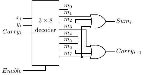
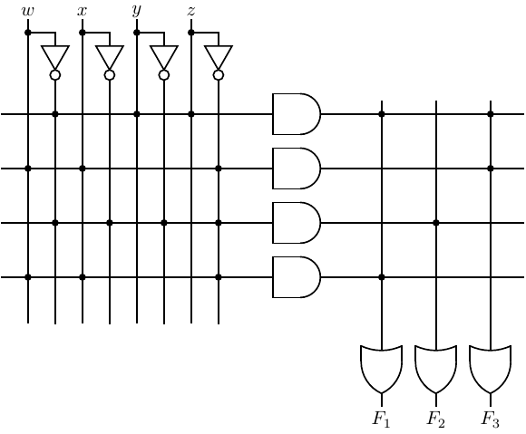
The 3 × 8 decoder specified in Table 5.2 can be implemented with 4-input AND gates as shown in Figure 5.6.
Decoders are more versatile than it might seem at first glance. Each possible input can be seen as a minterm. Since each output is one only when a particular minterm evaluates to one, a decoder can be viewed as a “minterm generator.” We know that any logical expression can be represented as the OR of minterms, so it follows that we can implement any logical expression by ORing the output(s) of a decoder.
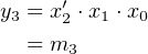
For example, let us rewrite Equation 5.1 for the Sum expression of a full adder using minterm notation (see Section 4.3.2):
 | (5.8) |
And for the Carry expression:
 | (5.9) |
where the subscripts on x, y, and Carry refer to the bit slice and the subscripts on m are part of the minterm notation. We can implement a full adder with a 3 × 8 decoder and two 4-input OR gates, as shown in Figure 5.7.
There are many places in the CPU where one of several signals must be selected to pass onward. For example, as you will see in Chapter 9, a value to be added by the ALU may come from a CPU register, come from memory, or actually be stored as part of the instruction itself. The device that allows this selection is essentially a switch.
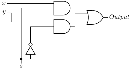
Figure 5.8 shows a multiplexer that can switch between two different inputs, x and y. The select input, s, determines which of the sources, either x or y, is passed on to the output. The action of this 2-way multiplexer is most easily seen in a truth table:
s | Output |
1 | x |
0 | y |
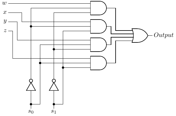
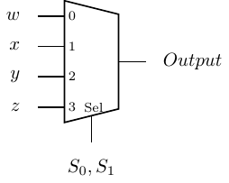
Here is a truth table for a multiplexer that can switch between four inputs, w, x, y, and z:
s1 | s0 | Output |
0 | 0 | w |
0 | 1 | x |
1 | 0 | y |
1 | 1 | z |
That is,
 | (5.10) |
which is implemented as shown in Figure 5.9.
The symbol for this multiplexer is shown in Figure 5.10.
Notice that the selection input, s, must be 2 bits in order to select between four inputs. In general, a 2n-way multiplexer requires an n-bit selection input.
Combinational logic circuits can be constructed from programmable logic devices (PLDs). The general idea is illustrated in Figure 5.11 for two input variables and two output functions of these variables.
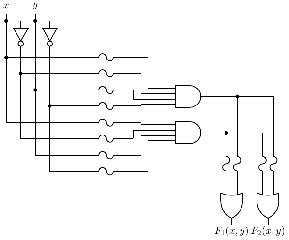
Each of the input variables, both in its uncomplemented and complemented form, are inputs to AND gates through fuses. (The “S” shaped lines in the circuit diagram represent fuses.) The fuses can be “blown” or left in place in order to program each AND gate to output a product. Since every input, plus its complement, is input to each AND gate, any of the AND gates can be programmed to output a minterm.
The products produced by the array of AND gates are all connected to OR gates, also through fuses. Thus, depending on which OR-gate fuses are left in place, the output of each OR gate is a sum of products. There may be additional logic circuitry to select between the different outputs. We have already seen that any Boolean function can be expressed as a sum of products, so this logic device can be programmed by “blowing” the fuses to implement any Boolean function.
PLDs come in many configurations. Some are pre-programmed at the time of manufacture. Others are programmed by the manufacturer. And there are types that can be programmed by a user. Some can even be erased and reprogrammed. Programming technologies range from specifying the manufacturing mask (for the pre-programmed devices) to inexpensive electronic programming systems. Some devices use “antifuses” instead of fuses. They are normally open. Programming such devices consists of completing the connection instead of removing it.
There are three general categories of PLDs:
We will now look at each category in more detail.
Programmable logic arrays are typically larger than the one shown in Figure 5.11, which is already complicated to draw. Figure 5.12 shows how PLAs are typically diagrammed.
This diagram deserves some explanation. Note in Figure 5.11 that each input variable and its complement is connected to the inputs of all the AND gates through a fuse. The AND gates have multiple inputs — one for each variable and its complement. Thus, the horizontal line leading to the inputs of the AND gates represent multiple wires. The diagram of Figure 5.12 has four input variables. So each AND gate has eight inputs, and the horizontal lines each represent the eight wires coming from the inputs and their complements.
The dots at the intersections of the vertical and horizontal line represent places where the fuses have been left intact. For example, the three dots on the topmost horizontal line indicate that there are three inputs to that AND gate The output of the topmost AND gate is
 |
Referring again to Figure 5.11, we see that the output from each AND gate is connected to each of the OR gates. Therefore, the OR gates also have multiple inputs — one for each AND gate — and the vertical lines leading to the OR gate inputs represent multiple wires. The PLA in Figure 5.12 has been programmed to provide the three functions:
 | (5.11) |
 | (5.12) |
 | (5.13) |
Read only memory can be implemented as a programmable logic device where only the OR plane can be programmed. The AND gate plane is wired to provide all the minterms. Thus, the inputs to the ROM can be thought of as addresses. Then the OR gate plane is programmed to provide the bit pattern at each address.
For example, the ROM diagrammed in Figure 5.13 has two inputs, a1 and a0.
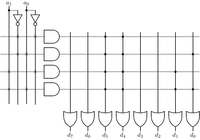
The AND gates are wired to give the minterms:
minterm | address |
a
1′a0′ | 00 |
a
1′a0 | 01 |
a1a0′ | 10 |
a1a0 | 11 |
And the OR gate plane has been programmed to store the four characters (in ASCII code):
minterm | address | contents |
a
1′a0′ | 00 | ′0′ |
a
1′a0 | 01 | ′1′ |
a1a0′ | 10 | ′2′ |
a1a0 | 11 | ′3′ |
You can see from this that the terminology “Read Only Memory” is perhaps a bit misleading. It is actually a combinational logic circuit. Strictly speaking, memory has a state that can be changed by inputs. (See Section 5.3.)
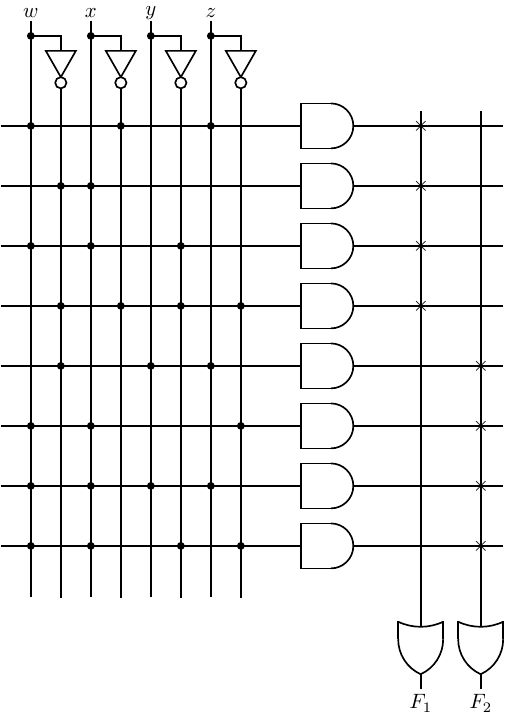
In a Programmable Array Logic (PAL) device, each OR gate is permanently wired to a group of AND gates. Only the AND gate plane is programmable. The PAL diagrammed in Figure 5.14 has four inputs. It provides two outputs, each of which can be the sum of up to four products. The “×” connections in the OR gate plane show that the top four AND gates are summed to produce F1 and the lower four to produce F2. The AND gate plane in this figure has been programmed to produce the two functions:
 | (5.14) |
 | (5.15) |
Combinational circuits (Section 5.1) are instantaneous (except for the time required for the electronics to settle). Their output depends only on the input at the time the output is observed. Sequential logic circuits, on the other hand, have a time history. That history is summarized by the current state of the circuit.
uniquely determines
This definition means that knowing the state of a system at a given time tells you everything you need to know in order to specify its behavior from that time on. How it got into this state is irrelevant.
This definition implies that the system has memory in which the state is stored. Since there are a finite number of states, the term finite state machine(FSM) is commonly used. Inputs to the system can cause the state to change.
If the output(s) depend only on the state of the FSM, it is called a Moore machine. And if the output(s) depend on both the state and the current input(s), it is called a Mealy machine.
The most commonly used sequential circuits are synchronous — their action is controlled by a sequence of clock pulses. The clock pulses are created by a clock generator circuit. The clock pulses are applied to all the sequential elements, thus causing them to operate in synchrony.
Asynchronous sequential circuits are not based on a clock. They depend upon a timing delay built into the individual elements. Their behavior depends upon the order in which inputs are applied. Hence, they are difficult to analyze and will not be discussed in this book.
A clock signal is typically a square wave that alternates between the 0 and 1 levels as shown in Figure 5.15 The amount of time spent at each level may be unequal. Although not a requirement, the timing pattern is usually uniform.
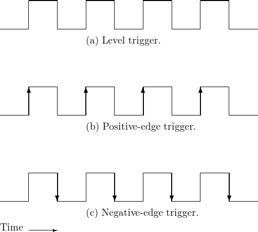
In Figure 5.15(a), the circuit operations take place during the entire time the clock is at the 1 level. As will be explained below, this can lead to unreliable circuit behavior. In order to achieve more reliable behavior, most circuits are designed such that a transition of the clock signal triggers the circuit elements to start their respective operations. Either a positive-going (Figure 5.15(b)) or negative-going (Figure 5.15(c)) transition may be used. The clock frequency must be slow enough such that all the circuit elements have time to complete their operations before the next clock transition (in the same direction) occurs.
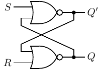
A latch is a storage device that can be in one of two states. That is, it stores one bit. It can be constructed from two or more gates connected such that feedback maintains the state as long as power is applied. The most fundamental latch is the SR (Set-Reset).
A simple implementation using NOR gates is shown in Figure 5.16.
When Q = 1 (⇔ Q′ = 0) it is in the Set state. When Q = 0 (⇔ Q′ = 1) it is in the Reset state.
There are four possible input combinations.
If Q = 0 and Q′ = 1, the output of the upper NOR gate is (0 + 0)′ = 1, and the output of the lower NOR gate is (1 + 0)′ = 0.
If Q = 1 and Q′ = 0, the output of the upper NOR gate is (0 + 1)′ = 0, and the output of the lower NOR gate is (0 + 0)′ = 1.
Thus, the cross feedback between the two NOR gates maintains the state — Set or Reset — of the latch.
If Q = 1 and Q′ = 0, the output of the upper NOR gate is (1 + 1)′ = 0, and the output of the lower NOR gate is (0 + 0)′ = 1. The latch remains in the Set state.
If Q = 0 and Q′ = 1, the output of the upper NOR gate is (1 + 0)′ = 0. This is fed back to the input of the lower NOR gate to give (0 + 0)′ = 1. The feedback from the output of the lower NOR gate to the input of the upper keeps the output of the upper NOR gate at (1 + 1)′ = 0. The latch has moved into the Set state.
If Q = 1 and Q′ = 0, the output of the lower NOR gate is (0 + 1)′ = 0. This causes the output of the upper NOR gate to become (0 + 0)′ = 1. The feedback from the output of the upper NOR gate to the input of the lower keeps the output of the lower NOR gate at (1 + 1)′ = 0. The latch has moved into the Reset state.
If Q = 0 and Q′ = 1, the output of the lower NOR gate is (1 + 1)′ = 0, and the output of the upper NOR gate is (0 + 0)′ = 1. The latch remains in the Reset state.
If Q = 0 and Q′ = 1, the output of the upper NOR gate is (1 + 0)′ = 0. This is fed back to the input of the lower NOR gate to give (0 + 1)′ = 0 as its output. The feedback from the output of the lower NOR gate to the input of the upper maintains its output as (1 + 0)′ = 0. Thus, Q = Q′ = 0, which is not allowed.
If Q = 1 and Q′ = 0, the output of the lower NOR gate is (0 + 1)′ = 0. This is fed back to the input of the upper NOR gate to give (1 + 0)′ = 0 as its output. The feedback from the output of the upper NOR gate to the input of the lower maintains its output as (0 + 1)′ = 0. Thus, Q = Q′ = 0, which is not allowed.
The state table in Table 5.3 summarizes the behavior of a NOR-based SR latch.
Current | Next | ||
S | R | State | State |
0 | 0 | 0 | 0 |
0 | 0 | 1 | 1 |
0 | 1 | 0 | 0 |
0 | 1 | 1 | 0 |
1 | 0 | 0 | 1 |
1 | 0 | 1 | 1 |
1 | 1 | 0 | X |
1 | 1 | 1 | X |
The inputs to a NOR-based SR latches are normally held at 0, which maintains the current state, Q. Its current state is available at the output. Momentarily changing S or R to 1 causes the state to change to Set or Reset, respectively, as shown in the Qnext column.
Notice that placing 1 on both the Set and Reset inputs at the same time causes a problem. Then the outputs of both NOR gates would become 0. In other words, Q = Q′ = 0, which is logically impossible. The circuit design must be such to prevent this input combination.
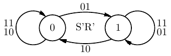
The behavior of an SR latch can also be shown by the state diagram in Figure 5.17
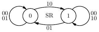
A state diagram is a directed graph. The circles show the possible states. Lines with arrows show the possible transitions between the states and are labeled with the input that causes the transition.
The two circles in Figure 5.17 show the two possible states of the SR latch — 0 or 1. The labels on the lines show the two-bit inputs, SR, that cause each state transition. Notice that when the latch is in state 0 there are two possible inputs, SR = 00 and SR = 01, that cause it to remain in that state. Similarly, when it is in state 1 either of the two inputs, SR = 00 or SR = 10, cause it to remain in that state.
The output of the SR latch is simply the state so is not shown separately on this state diagram. In general, if the output of a circuit is dependent on the input, it is often shown on the directed lines of the state diagram in the format “input/output.” If the output is dependent on the state, it is more common to show it in the corresponding state circle in “state/output” format.
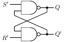
NAND gates are more commonly used than NOR gates, and it is possible to build an SR latch from NAND gates. Recalling that NAND and NOR have complementary properties, we will think ahead and use S′ and R′ as the inputs, as shown in Figure 5.18.
Consider the four possible input combinations.
If Q = 0 and Q′ = 1, the output of the upper NAND gate is (1 ⋅ 1)′ = 0, and the output of the lower NAND gate is (0 ⋅ 1)′ = 1.
If Q = 1 and Q′ = 0, the output of the upper NAND gate is (1 ⋅ 0)′ = 1, and the output of the lower NAND gate is (1 ⋅ 1)′ = 0.
Thus, the cross feedback between the two NAND gates maintains the state — Set or Reset — of the latch.
If Q = 1 and Q′ = 0, the output of the upper NAND gate is (0 ⋅ 0)′ = 1, and the output of the lower NAND gate is (1 ⋅ 1)′ = 0. The latch remains in the Set state.
If Q = 0 and Q′ = 1, the output of the upper NAND gate is (0 ⋅ 1)′ = 1. This causes the output of the lower NAND gate to become (1 ⋅ 1)′ = 0. The feedback from the output of the lower NAND gate to the input of the upper keeps the output of the upper NAND gate at (0 ⋅ 0)′ = 1. The latch has moved into the Set state.
If Q = 0 and Q′ = 1, the output of the lower NAND gate is (0 ⋅ 0)′ = 1, and the output of the upper NAND gate is (1 ⋅ 1)′ = 0. The latch remains in the Reset state.
If Q = 1 and Q′ = 0, the output of the lower NAND gate is (1 ⋅ 0)′ = 1. This is fed back to the input of the upper NAND gate to give (1 ⋅ 1)′ = 0. The feedback from the output of the upper NAND gate to the input of the lower keeps the output of the lower NAND gate at (0 ⋅ 0)′ = 1. The latch has moved into the Reset state.
If Q = 0 and Q′ = 1, the output of the upper NAND gate is (0 ⋅ 1)′ = 1. This is fed back to the input of the lower NAND gate to give (1 ⋅ 0)′ = 1 as its output. The feedback from the output of the lower NAND gate to the input of the upper maintains its output as (0 ⋅ 0)′ = 1. Thus, Q = Q′ = 1, which is not allowed.
If Q = 1 and Q′ = 0, the output of the lower NAND gate is (1 ⋅ 0)′ = 1. This is fed back to the input of the upper NAND gate to give (0 ⋅ 1)′ = 1 as its output. The feedback from the output of the upper NAND gate to the input of the lower maintains its output as (1 ⋅ 1)′ = 0. Thus, Q = Q′ = 1, which is not allowed.
Figure 5.19 shows the behavior of a NAND-based S’R’ latch. The inputs to a NAND-based S’R’ latch are normally held at 1, which maintains the current state, Q. Its current state is available at the output. Momentarily changing S′ or R′ to 0 causes the state to change to Set or Reset, respectively, as shown in the “Next State” column.
|
|
|
Notice that placing 0 on both the Set and Reset inputs at the same time causes a problem. Then the outputs of both NOR gates would become 0. In other words, Q = Q′ = 0, which is logically impossible. The circuit design must be such to prevent this input combination.
So the S’R’ latch implemented with two NAND gates can be thought of as the complement of the NOR gate SR latch. The state is maintained by holding both S′ and ′ at 1. S′ = 0 causes the state to be 1 (Set), and R′ = 0 causes the state to be 0 (Reset). Using S′ and R′ as the activating signals are usually called active-low signals.
You have already seen that ones and zeros are represented by either a high or low voltage in electronic logic circuits. A given logic device may be activated by combinations of the two voltages. To show which is used to cause activation at any given input, the following definitions are used:
An active-high signal can be connected to an active-low input, but the hardware designer must take the difference into account. For example, say that the required logical input is 1 to an active-low input. Since it is active-low, that means the required voltage is the lower of the two. If the signal to be connected to this input is active-high, then a logical 1 is the higher of the two voltages. So this signal must first be complemented in order to be interpreted as a 1 at the active-low input.
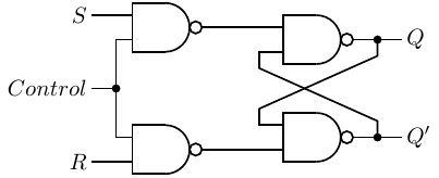
We can get better control over the SR latch by adding two NAND gates to provide a Control input, as shown in Figure 5.20.
In this circuit the outputs of both the control NAND gates remain at 1 as long as Control = 0. Table 5.4 shows the state behavior of the SR latch with control.
Current | Next | |||
Control | S | R | State | State |
0 | − | − | 0 | 0 |
0 | − | − | 1 | 1 |
1 | 0 | 0 | 0 | 0 |
1 | 0 | 0 | 1 | 1 |
1 | 0 | 1 | 0 | 0 |
1 | 0 | 1 | 1 | 0 |
1 | 1 | 0 | 0 | 1 |
1 | 1 | 0 | 1 | 1 |
1 | 1 | 1 | 0 | X |
1 | 1 | 1 | 1 | X |
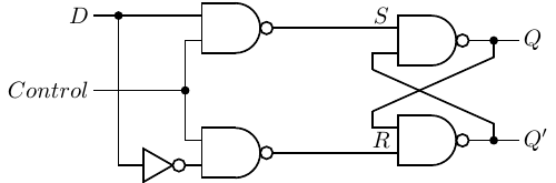
It is clearly better if we could find a design that eliminates the possibility of the “not allowed” inputs. Table 5.5 is a state table for a D latch. It has two inputs, one for control, the other for data, D. D = 1 sets the latch to 1, and D = 0 resets it to 0.
Current | Next | ||
Control | D | State | State |
0 | − | 0 | 0 |
0 | − | 1 | 1 |
1 | 0 | 0 | 0 |
1 | 0 | 1 | 0 |
1 | 1 | 0 | 1 |
1 | 1 | 1 | 1 |
The D latch can be implemented as shown in Figure 5.21.
The one data input, D, is fed to the “S” side of the SR latch; the complement of the data value is fed to the “R” side.
Now we have a circuit that can store one bit of data, using the D input, and can be synchronized with a clock signal, using the Control input. Although this circuit is reliable by itself, the issue is whether it is reliable when connected with other circuit elements. The D signal almost certainly comes from an interconnection of combinational and sequential logic circuits. If it changes while the Control is still 1, the state of the latch will be changed.
Each electronic element in a circuit takes time to activate. It is a very short period of time, but it can vary slightly depending upon precisely how the other logic elements are interconnected and the state of each of them when they are activated. The problem here is that the Control input is being used to control the circuit based on the clock signal level. The clock level must be maintained for a time long enough to allow all the circuit elements to complete their activity, which can vary depending on what actions are being performed. In essence, the circuit timing is determined by the circuit elements and their actions instead of the clock. This makes it very difficult to achieve a reliable design.
It is much easier to design reliable circuits if the time when an activity can be triggered is made very short. The solution is to use edge-triggered logic elements. The inputs are applied and enough time is allowed for the electronics to settle. Then the next clock transition activates the circuit element. This scheme provides concise timing under control of the clock instead of timing determined more or less by the particular circuit design.
Although the terminology varies somewhat in the literature, it is generally agreed that (see Figure 5.15.):
At each “tick” of the clock, there are four possible actions that might be taken on a single bit — store 0, store 1, complement the bit (also called toggle), or leave it as is.
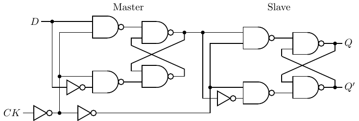
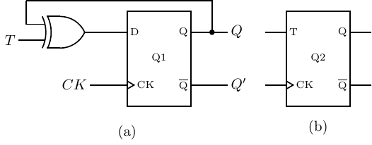
A D flip-flop is a common device for storing a single bit. We can turn the D latch into a D flip-flop by using two D latches connected in a master/slave configuration as shown in Figure 5.22.
Let us walk through the operation of this circuit.
The bit to be stored, 0 or 1, is applied to the D input of the Master D latch. The clock signal is applied to the CK input. It is normally 0. When the clock signal makes a transition from 0 to 1, the Master D latch will either Reset or Set, following the D input of 0 or 1, respectively.
While the CK input is at the 1 level, the control signal to the Slave D latch is 1, which deactivates this latch. Meanwhile, the output of this flip-flop, the output of the Slave D latch, is probably connected to the input of another circuit, which is activated by the same CK. Since the state of the Slave does not change during this clock half-cycle, the second circuit has enough time to read the current state of the flip-flop connected to its input. Also during this clock half-cycle, the state of the Master D latch has ample time to settle.
When the CK input transitions back to the 0 level, the control signal to the Master D latch becomes 1, deactivating it. At the same time, the control input to the Slave D latch goes to 0, thus activating the Slave D latch to store the appropriate value, 0 or 1. The new input will be applied to the Slave D latch during the second clock half-cycle, after the circuit connected to its output has had sufficient time to read its previous state. Thus, signals travel along a path of logic circuits in lock step with a clock signal.
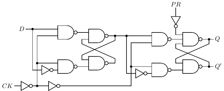
There are applications where a flip-flop must be set to a known value before the clocking begins. Figure 5.23 shows a D flip-flop with an asynchronous preset input added to it.
When a 1 is applied to the PR input, Q becomes 1 and Q′ 0, regardless of what the other inputs are, even CLK. It is also common to have an asynchronous clear input that sets the state (and output) to 0.
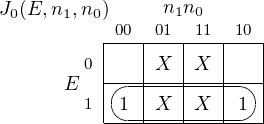
There are more efficient circuits for implementing edge-triggered D flip-flops, but this discussion serves to show that they can be constructed from ordinary logic gates. They are economical and efficient, so are widely used in very large scale integration circuits. Rather than draw the details for each D flip-flop, circuit designers use the symbols shown in Figure 5.24.
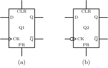
The various inputs and outputs are labeled in this figure. Hardware designers typically use Q instead of Q′. It is common to label the circuit as “Qn,” with n = 1, 2,…for identification. The small circle at the clock input in Figure 5.24(b) means that this D flip-flop is triggered by a negative-going clock transition. The D flip-flop circuit in Figure 5.22 can be changed to a negative-going trigger by simply removing the first NOT gate at the CK input.
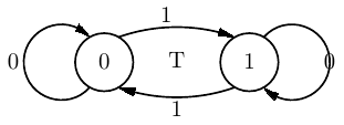
The flip-flop that simply complements its state, a T flip-flop, is easily constructed from a D flip-flop. The state table and state diagram for a T flip-flop are shown in Figure 5.25.
|
|
|
To determine the value that must be presented to the D flip-flop in order to implement a T flip-flop, we add a column for D to the state table as shown in Table 5.6.
Current | Next | ||
T | State | State | D |
0 | 0 | 0 | 0 |
0 | 1 | 1 | 1 |
1 | 0 | 1 | 1 |
1 | 1 | 0 | 0 |
By simply looking in the “Next State” column we can see what the input to the D flip-flop must be in order to obtain the correct state. These values are entered in the D column. (We will generalize this design procedure in Section 5.4.)
From Table 5.6 it is easy to write the equation for D:
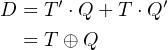 | (5.16) |
The resulting design for the T flip-flop is shown in Figure 5.26.
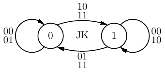
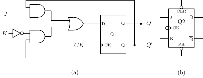
Implementing all four possible actions — set, reset, keep, toggle — requires two inputs, J and K, which leads us to the JK flip-flop. The state table and state diagram for a JK flip-flop are shown in Figure 5.27.
|
|
|
In order to determine the value that must be presented to the D flip-flop we add a column for D to the state table as shown in Table 5.7.
Current | Next | |||
J | K | State | State | D |
0 | 0 | 0 | 0 | 0 |
0 | 0 | 1 | 1 | 1 |
0 | 1 | 0 | 0 | 0 |
0 | 1 | 1 | 0 | 0 |
1 | 0 | 0 | 1 | 1 |
1 | 0 | 1 | 1 | 1 |
1 | 1 | 0 | 1 | 1 |
1 | 1 | 1 | 0 | 0 |
shows what values must be input to the D flip-flop. From this it is easy to write the equation for D:
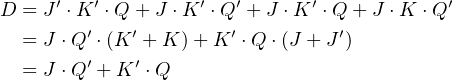 | (5.17) |
Thus, a JK flip-flop can be constructed from a D flip-flop as shown in Figure 5.28.
We will now consider a more general set of steps for designing sequential circuits.1 Design in any field is usually an iterative process, as you have no doubt learned from your programming experience. You start with a design, analyze it, and then refine the design to make it faster, less expensive, etc. After gaining some experience, the design process usually requires fewer iterations.
The following steps form a good method for a first working design:
Example 5-a ______________________________________________________________________________________________________
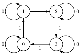
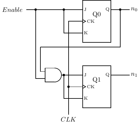
Design a counter that has an Enable input. When Enable = 1 it increments through the sequence 0, 1, 2, 3, 0, 1,…with each clock tick. Enable = 0 causes the counter to remain in its current state.
Solution:
|
|
At each clock tick the counter increments by one if Enable = 1. If Enable = 0 it remains in the current state. We have only shown the inputs because the output is equal to the state.
Enable = 0 | Enable = 1 | ||||
Current | Next | Next
| |||
n1 | n0 | n1 | n0 | n1 | n0 |
0 | 0 | 0 | 0 | 0 | 1 |
0 | 1 | 0 | 1 | 1 | 0 |
1 | 0 | 1 | 0 | 1 | 1 |
1 | 1 | 1 | 1 | 0 | 0 |
Enable = 0 | Enable = 1 | ||||||||||||
Current | Next | Next
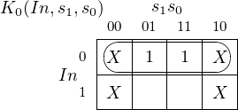
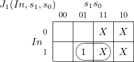
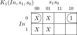
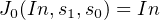
| |||||||||||
n1 | n0 | n1 | n0 | J1 | K1 | J0 | K0 | n1 | n0 | J1 | K1 | J0 | K0 |
0 | 0 | 0 | 0 | 0 | X | 0 | X | 0 | 1 | 0 | X | 1 | X |
0 | 1 | 0 | 1 | 0 | X | X | 0 | 1 | 0 | 1 | X | X | 1 |
1 | 0 | 1 | 0 | X | 0 | 0 | X | 1 | 1 | X | 0 | 1 | X |
1 | 1 | 1 | 1 | X | 0 | X | 0 | 0 | 0 | X | 1 | X | 1 |
Notice the “don’t care” entries in the state table. Since the JK flip-flop is so versatile, including the “don’t cares” helps find simpler circuit realizations. (See Exercise 5-3.)
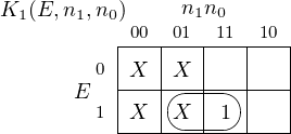
 |
 |
 |
 |
 |
The timing of the binary counter is shown here when counting through the sequence 3, 0, 1, 2, 3 (11,00,01,10,11).
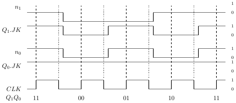
Qi .JK is the input to the ith JK flip-flop, and n i is its output. (Recall that J = K in this design.) When the ith input, Qi.JK, is applied to its JK flip-flop, remember that the state of the flip-flop does not change until the second half of the clock cycle. This can be seen when comparing the trace for the corresponding output, ni, in the figure.
Note the short delay after a clock transition before the value of each ni actually changes. This represents the time required for the electronics to completely settle to the new values.
__________________________________________________________________________________□
Except for very inexpensive microcontrollers, most modern CPUs execute instructions in stages. An instruction passes through each stage in an assembly-line fashion, called a pipeline. The action of the first stage is to fetch the instruction from memory, as will be explained in Chapter 6.
After an instruction is fetched from memory, it passes onto the next stage. Simultaneously, the first stage of the CPU fetches the next instruction from memory. The result is that the CPU is working on several instructions at the same time. This provides some parallelism, thus improving execution speed.
Almost all programs contain conditional branch points — places where the next instruction to be fetched can be in one of two different memory locations. Unfortunately, the decision of which of the two instructions to fetch is not known until the decision-making instruction has moved several stages into the pipeline. In order to maintain execution speed, as soon as a conditional branch instruction has passed on from the fetch stage, the CPU needs to predict where to fetch the next instruction from.
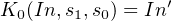
In this next example we will design a circuit to implement a prediction circuit.
Example 5-b ______________________________________________________________________________________________________
Design a circuit that predicts whether a conditional branch is taken or not. The predictor continues to predict the same outcome, take the branch or do not take the branch, until it makes two mistakes in a row.
Solution:
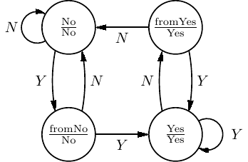
Let us begin in the “No” state. The prediction is that the next branch will also not be taken.
The notation in the state bubbles is  , showing that the output in this state is also
“No.”
, showing that the output in this state is also
“No.”
The input to the circuit is whether or not the branch was actually taken. The arc labeled “N” shows the transition when the branch was not taken. It loops back to the “No” state, with the prediction (the output) that the branch will not be taken the next time. If the branch is taken, the “Y” arc shows that the circuit moves into the “fromNo” state, but still predicting no branch the next time.
From the “fromNo” state, if the branch is not taken (the prediction is correct), the circuit returns to the “No” state. However, if the branch is taken, the “Y” shows that the circuit moves into the “Yes” state. This means that the circuit predicted incorrectly twice in a row, so the prediction is changed to “Yes.”
You should be able to follow this state diagram for the other cases and convince yourself that both the “fromNo” and “fromYes” states are required.
Taken = No | Taken = Y es | ||||
Current | Next | Next
| |||
State | Prediction | State | Prediction | State | Prediction |
No | No | No | No | fromNo | No |
fromNo | No | No | No | Y es | Y es |
fromY es | Y es | No | No | Y es | Y es |
Y es | Y es | fromY es | Y es | Y es | Y es |
Since there are four states, we need two bits. We will let 0 represent “No” and 1 represent “Yes.” The input is whether the branch is actually taken (1) or not (0). And the output is the prediction of whether it will be taken (1) or not (0).
We choose a binary code for the state, s1s0, such that the high-order bit represents the prediction, and the low-order bit what the last input was. That is:
State | Prediction | s1 | s0 |
No | No | 0 | 0 |
fromNo | No | 0 | 1 |
fromY es | Y es | 1 | 0 |
Y es | Y es | 1 | 1 |
This leads to the state table in binary:
Input = 0 | Input = 1
| ||||
Current | Next | Next | |||
s
1 | s0 | s1 | s0 | s1 | s0 |
0 | 0 | 0 | 0 | 0 | 1 |
0 | 1 | 0 | 0 | 1 | 1 |
1 | 0 | 0 | 0 | 1 | 1 |
1 | 1 | 1 | 0 | 1 | 1 |
Input = 0 | Input = 1
| ||||||||||||
Current | Next | Next | |||||||||||
s
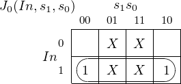
1 | s0 | s1 | s0 | J1 | K1 | J0 | K0 | s1 | s0 | J1 | K1 | J0 | K0 |
0 | 0 | 0 | 0 | 0 | X | 0 | X | 0 | 1 | 0 | X | 1 | X |
0 | 1 | 0 | 0 | 0 | X | X | 1 | 1 | 1 | 1 | X | X | 0 |
1 | 0 | 0 | 0 | X | 1 | 0 | X | 1 | 1 | X | 0 | 1 | X |
1 | 1 | 1 | 0 | X | 0 | X | 1 | 1 | 1 | X | 0 | X | 0 |
 |
 |
 |
 |
In this section we will discuss how registers, SRAM, and DRAM are organized and constructed. Keeping with the intent of this book, the discussion will be introductory only.
Registers are used in places where small amounts of very fast memory is required. Many are found in the CPU where they are used for numerical computations, temporary data storage, etc. They are also used in the hardware that serves to interface between the CPU and other devices in the computer system.
We begin with a simple 4-bit register, which allows us to store four bits. Figure 5.29 shows a design for implementing a 4-bit register using D flip-flops.
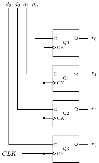
As described above, each time the clock cycles the state of each of the D flip-flops is set according to the value of d = d3d2d1d0. The problem with this circuit is that any changes in any of the dis will change the state of the corresponding bit in the next clock cycle, so the contents of the register are essentially valid for only one clock cycle.
One-cycle buffering of a bit pattern is sufficient for some applications, but there is also a need for registers that will store a value until it is explicitly changed, perhaps billions of clock cycles later. The circuit in Figure 5.30 uses adds a load signal and feedback from the output of each bit. When load = 1 each bit is set according to its corresponding input, di. When load = 0 the output of each bit, ri, is used as the input, giving no change.
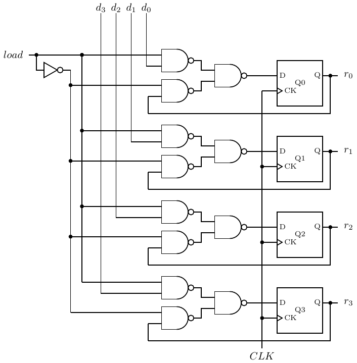
So this register can be used to store a value for as many clock cycles as desired. The value will not be changed until load is set to 1.
Most computers need many general purpose registers. When two or more registers are grouped together, the unit is called a register file. A mechanism must be provided for addressing one of the registers in the register file.
Consider a register file composed of eight 4-bit registers, r0 – r7. We could build eight copies of the circuit shown in Figure 5.30. Let the 4-bit data input, d, be connected in parallel to all of the corresponding data pins, d3d2d1d0, of each of the eight registers. Three bits are required to address one of the registers (23 = 8). If the 8-bit output from a 3 × 8 decoder is connected to the eight load inputs of each of the registers, d will be loaded into one, and only one, of the registers during the next clock cycle. All the other registers will have load = 0, and they will simply maintain their current state. Selecting the output from one of the eight registers can be done with four 8-input multiplexers. One such multiplexer is shown in Figure 5.31. The inputs r0i – r7i are the ith bits from each of eight registers, r0 – r7.
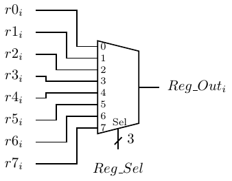
One of the eight registers is selected for the 1-bit output, Reg_Outi, by the 3-bit input Reg_Sel. Keep in mind that four of these output circuits would be required for 4-bit registers. The same Reg_Sel would be applied to all four multiplexers simultaneously in order to output all four bits of the same register. Larger registers would, of course, require correspondingly more multiplexers.
There is another important feature of this design that follows from the master/slave property of the D flip-flops. The state of the slave portion does not change until the second half of the clock cycle. So the circuit connected to the output of this register can read the current state during the first half of the clock cycle, while the master portion is preparing to change the state to the new contents.
There are many situations where it is desirable to shift a group of bits. A shift register is a common device for doing this. Common applications include:
Serial-to-parallel and parallel-to-serial conversion is required in I/O controllers because most I/O communication is serial bit streams, while data processing in the CPU is performed on groups of bits in parallel.
A simple 4-bit serial-to-parallel shift register is shown in Figure 5.32.
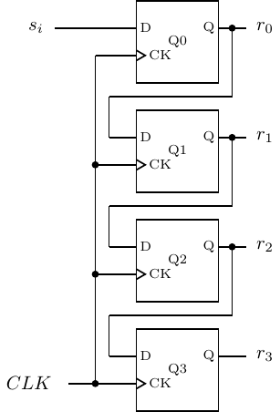
A serial stream of bits is input at si. At each clock tick, the output of Q0 is applied to the input of Q1, thus copying the previous value of r0 to the new r1. The state of Q0 changes to the value of the new si, thus copying this to be the new value of r0. The serial stream of bits continues to ripple through the four bits of the shift register. At any time, the last four bits in the serial stream are available in parallel at the four outputs, r3,…,r0.
The same circuit could be used to provide a time delay of four clock ticks in a serial bit stream. Simply use r3 as the serial output.
There are several problems with trying to extend this design to large memory systems. First, although a multiplexer works for selecting the output from several registers, one that selects from a many million memory cells is simply too large. From Figure 5.9 (page 333), we see that such a multiplexer would need an AND gate for each memory cell, plus an OR gate with an input for each of these millions of AND gate outputs.
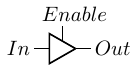
We need another logic element called a tri-state buffer. The tri-state buffer has three possible outputs — 0, 1, and “high Z.” “High Z” describes a very high impedance connection (see Section 4.4.2, page 237.) It can be thought of as essentially “no connection” or “open.”
It takes two inputs — data input and enable. The truth table describing a tri-state buffer is:
Enable | In | Out |
0 | 0 | highZ |
0 | 1 | highZ |
1 | 0 | 0 |
1 | 1 | 1 |
and its circuit symbol is shown in Figure 5.33.
When Enable = 1 the output, which is equal to the input, is connected to whatever circuit element follows the tri-state buffer. But when Enable = 0, the output is essentially disconnected. Be careful to realize that this is different from 0; being disconnected means it has no effect on the circuit element to which it is connected.
A 4-way multiplexer using a 2 × 4 decoder and four tri-state buffers is illustrated in Figure 5.34.
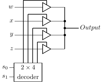
Compare this design with the 4-way multiplexer shown in Figure 5.9, page 333. The tri-state buffer design may not be an advantage for small multiplexers. But an n-way multiplexer without tri-state buffers requires an n-input OR gate, which presents some technical electronic problems.
Figure 5.35 shows how tri-state buffers can be used to implement a single memory cell.
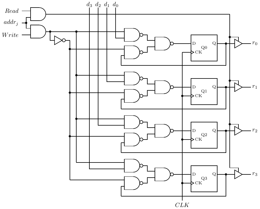
This circuit shows only one 4-bit memory cell so you can compare it with the register design in Figure 5.29, but it scales to much larger memories. Write is asserted to store data in the D flip-flops. Read enables the output tri-state buffer in order to connect the single output line to Mem_data_out. The address decoder is also used to enable the tri-state buffers to connect a memory cell to the output, r3r2r1r0.
This type of memory is called Static Random Access Memory (SRAM). “Static” because the memory retains its stored values as long as power to the circuit is maintained. “Random access” because it takes the same length of time to access the memory at any address.
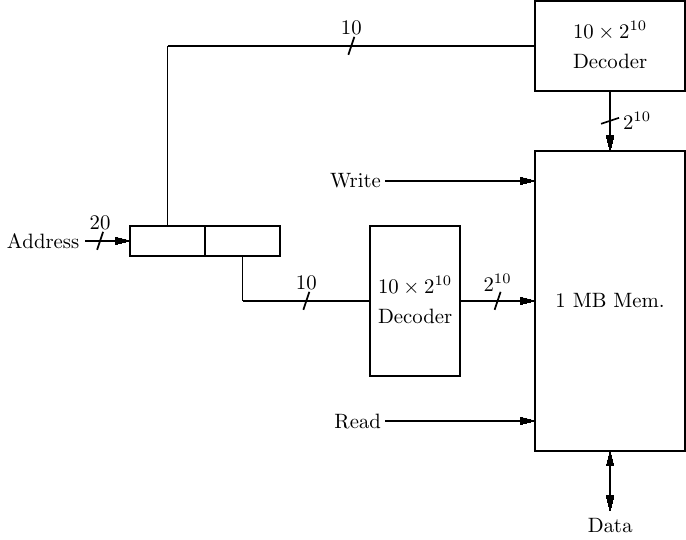
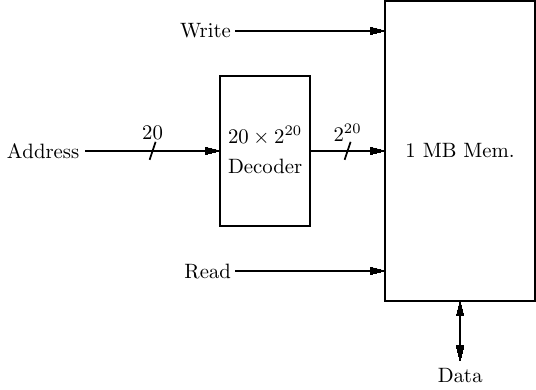
A 1 MB memory requires a 20 bit address. This requires a 20 × 220 address decoder as shown in Figure 5.36.
Recall from Section 5.1.3 (page 318) that an n × 2n decoder requires 2n AND gates. We can simplify the circuitry by organizing memory into a grid of rows and columns as shown in Figure 5.37.
Although two decoders are required, each requires 2n∕2 AND gates, for a total of 2 × 2n∕2 = 2(n∕2)+1 AND gates for the decoders. Of course, memory cell access is slightly more complex, and some complexity is added in order to split the 20-bit address into two 10-bit portions.
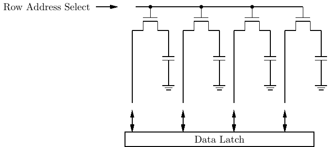
Each bit in SRAM requires about six transistors for its implementation. A less expensive solution is found in Dynamic Random Access Memory (DRAM). In DRAM each bit value is stored by a charging a capacitor to one of two voltages. The circuit requires only one transistor to charge the capacitor, as shown in Figure 5.38.
This Figure shows only four bits in a single row.
When the “Row Address Select” line is asserted all the transistors in that row are turned on, thus connecting the respective capacitor to the Data Latch. The value stored in the capacitor, high voltage or low voltage, is stored in the Data Latch. There, it is available to be read from the memory. Since this action tends to discharge the capacitors, they must be refreshed from the values stored in the Data Latch.
When new data is to be stored in DRAM, the current values are first stored in the Data Latch, just as in a read operation. Then the appropriate changes are made in the Data Latch before the capacitors are refreshed.
These operations take more time than simply switching flip-flops, so DRAM is appreciably slower than SRAM. In addition, capacitors lose their charge over time. So each row of capacitors must be read and refreshed in the order of every 60 msec. This requires additional circuitry and further slows memory access. But the much lower cost of DRAM compared to SRAM warrants the slower access time.
This has been only an introduction to how switching transistors can be connected into circuits to create a CPU. We leave the details to more advanced books, e.g., [20], [23], [24], [28], [31], [34].
The greatest benefit will be derived from these exercises if you either build the circuits with hardware or using a simulation program. Several free circuit simulation applications are available that run under GNU/Linux.
(§5.1) Build a four-bit adder.
(§5.1) Build a four-bit adder/subtracter.
(§5.4) Redesign the 2-bit counter of Example 5-a using only the “set” and “reset” inputs of the JK flip-flops. So your state table will not have any “don’t cares.”
(§5.4) Design a 4-bit up counter — 0, 1, 2,…,15, 0,…
(§5.4) Design a 4-bit down counter — 15, 14, 13,…,0, 15,…
(§5.4) Design a decimal counter — 0, 1, 2,…,9, 0,…
(§5.5) Build the register file described in Section 5.5.1. It has eight 4-bit registers. A 3 × 8 decoder is used to select a register to be loaded. Four 8-way multiplexers are used to select the four bits from one register to be output.