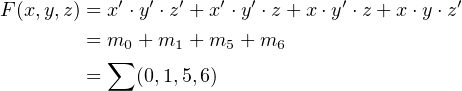
Chapter 4
Logic Gates
This chapter provides an overview of the hardware components that are used to build a computer. We will
limit the discussion to electronic computers, which use transistors to switch between two different voltages.
One voltage represents 0, the other 1. The hardware devices that implement the logical operations are called
logic gates.
4.1 Boolean Algebra
In order to understand how the components are combined to build a computer, you need to
learn another algebra system — Boolean algebra. There are many approaches to learning about
Boolean algebra. Some authors start with the postulates of Boolean algebra and develop the
mathematical tools needed for working with switching circuits from them. We will take the more
pragmatic approach of starting with the basic properties of Boolean algebra, then explore the
properties of the algebra. For a more theoretical approach, including discussions of more general
Boolean algebra concepts, search the internet, or take a look at books like [9], [20], [23], or
[24].
There are only two values, 0 and 1, unlike elementary algebra that deals with an infinity of values, the
real numbers. Since there are only two values, a truth table is a very useful tool for working with
Boolean algebra. A truth table lists all possible combinations of the variables in the problem. The
resulting value of the Boolean operation(s) for each variable combination is shown on the respective
row.
Elementary algebra has four operations, addition, subtraction, multiplication, and division, but Boolean
algebra has only three operations:
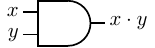
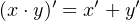
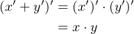
- AND — a binary operator; the result is 1 if and only if both operands are 1; otherwise the result is 0.
We will use ’⋅’ to designate the AND operation. It is also common to use the ’∧’ symbol
or simply “AND”. The hardware symbol for the AND gate is shown in Figure 4.1. The
inputs are x and y. The resulting output, x ⋅ y, is shown in the truth table in this figure.
We can see from the truth table that the AND operator follows similar rules as multiplication in
elementary algebra.
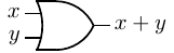
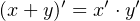
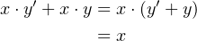
- OR — a binary operator; the result is 1 if at least one of the two operands is 1; otherwise the
result is 0. We will use ’+’ to designate the OR operation. It is also common to use the ’∨’
symbol or simply “OR”. The hardware symbol for the OR gate is shown in Figure 4.2. The
inputs are x and y. The resulting output, x + y, is shown in the truth table in this figure.
From the truth table we can see that the OR operator follows the same rules as addition in elementary
algebra except that
1 + 1 = 1
in Boolean algebra. Unlike elementary algebra, there is no carry from the OR operation. Since addition
of integers can produce a carry, you will see in Section 5.1 that implementing addition requires more
than a simple OR gate.
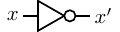
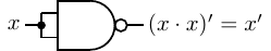
- NOT — a unary operator; the result is 1 if the operand is 0, or 0 if the operand is 1. Other names for
the NOT operation are complement and invert. We will use x′ to designate the NOT operation.
It is also common to use ¬x, or x. The hardware symbol for the NOT gate is shown in
Figure 4.3. The input is x. The resulting output, x′, is shown in the truth table in this
figure.
The NOT operation has no analog in elementary algebra. Be careful to notice that inversion of
a value in elementary algebra is a division operation, which does not exist in Boolean
algebra.
Two-state variables can be combined into expressions with these three operators in the same way that
you would use the C/C++ operators &&, ||, and ! to create logical expressions commonly used to control if
and while statements. We now examine some Boolean algebra properties for manipulating such expressions.
As you read through this material, keep in mind that the same techniques can be applied to logical
expressions in programming languages.
These properties are commonly presented as theorems. They are easily proved from application of truth
tables.
There is a duality between the AND and OR operators. In any equality you can interchange AND and
OR along with the constants 0 and 1, and the equality still holds. Thus the properties will be presented in
pairs that illustrate their duality. We first consider properties that are the same as in elementary
algebra.
Now we consider properties where Boolean algebra differs from elementary algebra.
- AND and OR are commutative:
 | (4.5) |
 | (4.6) |
This is easily proved by looking at the second and third lines of the respective truth tables. In
elementary algebra, only the addition and multiplication operators are commutative.
- AND and OR have a null value:
 | (4.7) |
 | (4.8) |
The null value for the AND is the same as multiplication in elementary algebra. But addition in
elementary algebra does not have a null constant, while OR in Boolean algebra does.
- AND and OR have a complement value:
 | (4.9) |
 | (4.10) |
Complement does not exist in elementary algebra.
- AND and OR are idempotent:
 | (4.11) |
 | (4.12) |
That is, repeated application of either operator to the same value does not change it. This differs
considerably from elementary algebra — repeated application of addition is equivalent to
multiplication and repeated application of multiplication is the power operation.
- AND and OR are distributive:
 | (4.13) |
 | (4.14) |
Going from right to left in Equation 4.13 is the very familiar factoring from addition and
multiplication in elementary algebra. On the other hand, the operation in Equation 4.14 has no analog
in elementary algebra. It follows from the idempotency property. The NOT operator has an obvious
property:
- NOT shows involution:
 | (4.15) |
Again, since there is no complement in elementary algebra, there is no equivalent property.
- DeMorgan’s Law is an important expression of the duality between the AND and OR
operations.
 | (4.16) |
 | (4.17) |
The validity of DeMorgan’s Law can be seen in the following truth tables. For Equation
4.16:
x | y | (x ⋅ y) | (x ⋅ y)′ | x′ | y′ | x′ + y′ |
|
|
|
|
|
|
|
0 | 0 | 0 | 1 | 1 | 1 | 1 |
0 | 1 | 0 | 1 | 1 | 0 | 1 |
1 | 0 | 0 | 1 | 0 | 1 | 1 |
1 | 1 | 1 | 0 | 0 | 0 | 0 |
|
And for Equation 4.17:
x | y | (x + y) | (x + y)′ | x′ | y′ | x′⋅ y′ |
|
|
|
|
|
|
|
0 | 0 | 0 | 1 | 1 | 1 | 1 |
0 | 1 | 1 | 0 | 1 | 0 | 0 |
1 | 0 | 1 | 0 | 0 | 1 | 0 |
1 | 1 | 1 | 0 | 0 | 0 | 0 |
|
4.2 Canonical (Standard) Forms
Some terminology and definitions at this point will help our discussion. Consider two dictionary definitions
of literal[26]:
| | literal | 1b: | adhering to fact or to the ordinary construction or primary
meaning of a term or expression : ACTUAL. |
| | | 2: | of, relating to, or expressed in letters. |
In programming we use the first definition of literal. For example, in the following code sequence
int xyz = 123; char a = ’b’; char *greeting = "Hello";
the number “123”, the character ‘b’, and the string “Hello” are all literals. They are interpreted by the
compiler exactly as written. On the other hand, “xyz”, “a”, and “greeting” are all names of
variables.
In mathematics we use the second definition of literal. That is, in the algebraic expression
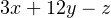
the letters x,y, and z are called literals. Furthermore, it is common to omit the “⋅” operator to designate
multiplication. Similarly, it is often dropped in Boolean algebra expressions when the AND operation is
implied.
The meaning of literal in Boolean algebra is slightly more specific.
-
literal
- A presence of a variable or its complement in an expression. For example, the expression
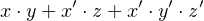
contains seven literals.
From the context of the discussion you should be able to tell which meaning of “literal” is intended and when
the “⋅” operator is omitted.
A Boolean expression is created from the numbers 0 and 1, and literals. Literals can be combined using
either the “⋅” or the “+” operators, which are multiplicative and additive operations, respectively. We will
use the following terminology.
-
product term:
- A term in which the literals are connected with the AND operator. AND is
multiplicative, hence the use of “product.”
-
minterm or standard product:
- A product term that contains each of the variables in the
problem, either in its complemented or uncomplemented form. For example, if a problem involves
three variables (say, x, y, and z), x ⋅ y ⋅ z, x′⋅ y ⋅ z′, and x′⋅ y′⋅ z′ are all minterms, but x ⋅ y is
not.
-
sum of products (SoP):
- One or more product terms connected with OR operators. OR is additive,
hence the use of “sum.”
-
sum of minterms (SoM) or canonical sum:
- An SoP in which each product term is a minterm.
Since all the variables are present in each minterm, the canonical sum is unique for a given
problem.
When first defining a problem, starting with the SoM ensures that the full effect of each variable has
been taken into account. This often does not lead to the best implementation. In Section 4.3 we will see
some tools to simplify the expression, and hence, the implementation.
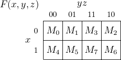
It is common to index the minterms according to the values of the variables that would cause that
minterm to evaluate to 1. For example, x′⋅y′⋅z′ = 1 when x = 0, y = 0, and z = 0, so this would be m0. The
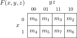
minterm x′⋅y ⋅z′ evaluates to 1 when x = 0, y = 1, and z = 0, so is m2. Table 4.1 lists all the minterms for a
three-variable expression.
minterm | x | y | z |
|
|
|
|
m0 = x′⋅ y′⋅ z′ | 0 | 0 | 0 |
m1 = x′⋅ y′⋅ z | 0 | 0 | 1 |
m2 = x′⋅ y ⋅ z′ | 0 | 1 | 0 |
m3 = x′⋅ y ⋅ z | 0 | 1 | 1 |
m4 = x ⋅ y′⋅ z′ | 1 | 0 | 0 |
m5 = x ⋅ y′⋅ z | 1 | 0 | 1 |
m6 = x ⋅ y ⋅ z′ | 1 | 1 | 0 |
m7 = x ⋅ y ⋅ z | 1 | 1 | 1 |
|
Table 4.1: Minterms for three variables. mi is the ith minterm. The x, y, and z values cause the
corresponding minterm to evaluate to 1.
A convenient notation for expressing a sum of minterms is to use the ∑
symbol with a numerical list of
the minterm indexes. For example,
 | (4.18) |
As you might expect, each of the terms defined above has a dual definition.
-
sum term:
- A term in which the literals are connected with the OR operator. OR is additive, hence
the use of “sum.”
-
maxterm or standard sum:
- A sum term that contains each of the variables in the problem, either
in its complemented or uncomplemented form. For example, if an expression involves three
variables, x, y, and z, (x + y + z), (x′ + y + z′), and (x′ + y′ + z′) are all maxterms, but (x + y)
is not.
-
product of sums (PoS):
- One or more sum terms connected with AND operators. AND is
multiplicative, hence the use of “product.”
-
product of maxterms (PoM) or canonical product:
- A PoS in which each sum term is a
maxterm. Since all the variables are present in each maxterm, the canonical product is unique
for a given problem.
It also follows that any Boolean function can be uniquely expressed as a product of maxterms (PoM)
that evaluate to 1. Starting with the product of maxterms ensures that the full effect of each variable has
been taken into account. Again, this often does not lead to the best implementation, and in Section 4.3 we
will see some tools to simplify PoMs.
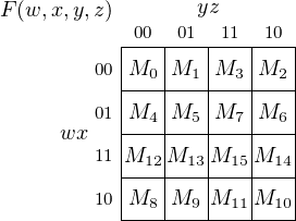
It is common to index the maxterms according to the values of the variables that would cause that
maxterm to evaluate to 0. For example, x + y + z = 0 when x = 0, y = 0, and z = 0, so this would be M0.
The maxterm x′ + y + z′ evaluates to 0 when x = 1, y = 0, and z = 1, so is m5. Table 4.2 lists all the
maxterms for a three-variable expression.
Maxterm | x | y | z |
|
|
|
|
M0 = x + y + z | 0 | 0 | 0 |
M1 = x + y + z′ | 0 | 0 | 1 |
M2 = x + y′ + z | 0 | 1 | 0 |
M3 = x + y′ + z′ | 0 | 1 | 1 |
M4 = x′ + y + z | 1 | 0 | 0 |
M5 = x′ + y + z′ | 1 | 0 | 1 |
M6 = x′ + y′ + z | 1 | 1 | 0 |
M7 = x′ + y′ + z′ | 1 | 1 | 1 |
|
Table 4.2: Maxterms for three variables. Mi is the ith maxterm. The x, y, and z values cause the
corresponding maxterm to evaluate to 0.
The similar notation for expressing a product of maxterms is to use the ∏
symbol with a numerical list
of the maxterm indexes. For example (and see Exercise 4-8),
 | (4.19) |
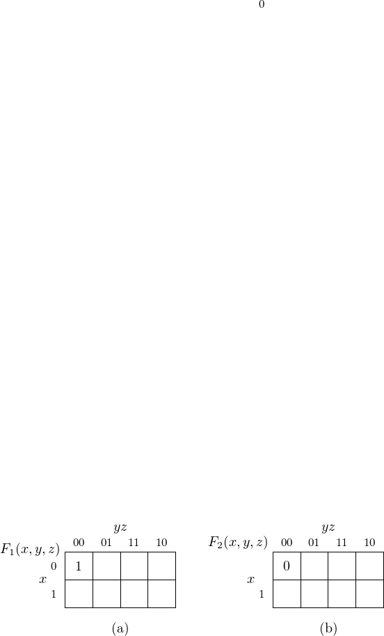
The names “minterm” and “maxterm” may seem somewhat arbitrary. But consider the two
functions,
 | (4.20) |
 | (4.21) |
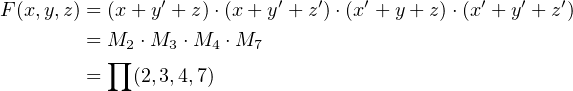
There are eight (23) permutations of the three variables, x, y, and z. F
1 has one minterm and evaluates to 1
for only one of the permutations, x = y = z = 1. F2 has one maxterm and evaluates to 1 for all permutations
except when x = y = z = 0. This is shown in the following truth table:
| | | minterm | maxterm |
x | y | z | F1 = (x ⋅ y ⋅ z) | F2 = (x + y + z) |
|
|
|
|
|
0 | 0 | 0 | 0 | 0 |
0 | 0 | 1 | 0 | 1 |
0 | 1 | 0 | 0 | 1 |
0 | 1 | 1 | 0 | 1 |
1 | 0 | 0 | 0 | 1 |
1 | 0 | 1 | 0 | 1 |
1 | 1 | 0 | 0 | 1 |
1 | 1 | 1 | 1 | 1 |
|
ORing more minterms to an SoP expression expands the number of cases where it evaluates to 1, and
ANDing more maxterms to a PoS expression reduces the number of cases where it evaluates to
1.
4.3 Boolean Function Minimization
In this section we explore some important tools for manipulating Boolean expressions in order to simplify
their hardware implementation. When implementing a Boolean function in hardware, each “⋅” operator
represents an AND gate and each “+” operator an OR gate. In general, the complexity of the hardware is
related to the number of AND and OR gates. NOT gates are simple and tend not to contribute significantly
to the complexity.
We begin with some definitions.
-
minimal sum of products (mSoP):
- A sum of products expression is minimal if all other mathematically
equivalent SoPs
- have at least as many product terms, and
- those with the same number of product terms have at least as many literals.
-
minimal product of sums (mPoS):
- A product of sums expression is minimal if all other mathematically
equivalent PoSs
- have at least as many sum factors, and
- those with the same number of sum factors have at least as many literals.
These definitions imply that there can be more than one minimal solution to a problem. Good hardware
design practice involves finding all the minimal solutions, then assessing each one within the context of the
available hardware. For example, judiciously placed NOT gates can actually reduce hardware complexity
(Section 4.4.3, page 260).
4.3.1 Minimization Using Algebraic Manipulations
To illustrate the importance of reducing the complexity of a Boolean function, consider the following
function:
 | (4.22) |
The expression on the right-hand side is an SoM. The circuit to implement this function is shown in Figure
4.4.
It requires three AND gates, one OR gate, and two NOT gates.
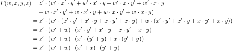
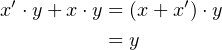
Now let us simplify the expression in Equation 4.22 to see if we can reduce the hardware requirements.
This process will probably seem odd to a person who is not used to manipulating Boolean expressions,
because there is not a single correct path to a solution. We present one way here. First we use
the idempotency property (Equation 4.12) to duplicate the third term, and then rearrange a
bit:
 | (4.23) |
Next we use the distributive property (Equation 4.13) to factor the expression:
 | (4.24) |
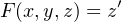
And from the complement property (Equation 4.10) we get:
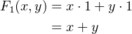 | (4.25) |
which you recognize as the simple OR operation. It is easy to see that this is a minimal sum of
products for this function. We can implement Equation 4.22 with a single OR gate — see Figure
4.2 on page 167. This is clearly a less expensive, faster circuit than the one shown in Figure
4.4.
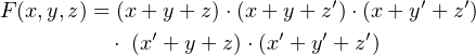
To illustrate how a product of sums expression can be minimized, consider the function:
 | (4.26) |
The expression on the right-hand side is a PoM. The circuit for this function is shown in Figure 4.5.
It requires three OR gates, one AND gate, and two NOT gates.
We will use the distributive property (Equation 4.14) on the right two factors and recognize the
complement (Equation 4.9):
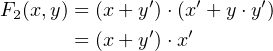 | (4.27) |
Now, use the distributive (Equation 4.13) and complement (Equation 4.9) properties to obtain:
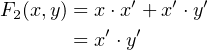 | (4.28) |
Thus, the function can be implemented with two NOT gates and a single AND gate, which is clearly a
minimal product of sums. Again, with a little algebraic manipulation we have arrived at a much simpler
solution.
Example 4-a ______________________________________________________________________________________________________
Design a function that will detect the even 4-bit integers.
Solution:
The even 4-bit integers are given by the function:
Using the distributive property repeatedly we get:
And from the complement property we arrive at a minimal sum of products:
__________________________________________________________________________________□
4.3.2 Minimization Using Graphic Tools
The Karnaugh map was invented in 1953 by Maurice Karnaugh while working as a telecommunications
engineer at Bell Labs. Also known as a K-map, it provides a graphic view of all the possible minterms for a
given number of variables. The format is a rectangular grid with a cell for each minterm. There are 2n cells
for n variables.
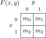
Figure 4.6 shows how all four minterms for two variables are mapped onto a four-cell Karnaugh map.
The vertical axis is used for plotting x and the horizontal for y. The value of x for each row is shown by
the number (0 or 1) immediately to the left of the row, and the value of y for each column appears at the top
of the column. Although it occurs automatically in a two-variable Karnaugh map, the cells must be arranged
such that only one variable changes between two cells that share an edge. This is called the adjacency
property.
The procedure for simplifying an SoP expression using a Karnaugh map is:
- Place a 1 in each cell that corresponds to a minterm that evaluates to 1 in the expression.
- Combine cells with 1s in them and that share edges into the largest possible groups. Larger
groups result in simpler expressions. The number of cells in a group must be a power of 2. The
edges of the Karnaugh map are considered to wrap around to the other side, both vertically
and horizontally.
- Groups may overlap. In fact, this is common. However, no group should be fully enclosed by
another group.
- The result is the sum of the product terms that represent each group.
The Karnaugh map provides a graphical means to find the same simplifications as algebraic
manipulations, but some people find it easier to spot simplification patterns on a Karnaugh map. Probably
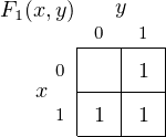
the easiest way to understand how Karnaugh maps are used is through an example. We start with Equation
4.22 (repeated here):
and use a Karnaugh map to graphically find the same minimal sum of products that the algebraic steps in
Equations 4.23 through 4.25 gave us.
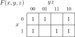
We start by placing a 1 in each cell corresponding to a minterm that appears in the equation as shown in
Figure 4.7.
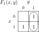
The two cells on the right side correspond to the minterms m1 and m3 and represent x′⋅ y + x ⋅ y.
Using the distributive (Equation 4.13) and complement (Equation 4.10) properties, we can see
that
 | (4.29) |
The simplification in Equation 4.29 is shown graphically by the grouping in Figure 4.8.
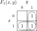
Since groups can overlap, we create a second grouping as shown in Figure 4.9. This grouping shows the
simplification,
 | (4.30) |
The group in the bottom row represents the product term x, and the one in the right-hand column
represents y. So the simplification is:
 | (4.31) |
Note that the overlapping cell, x ⋅ y, is the term that we used the idempotent property to duplicate in
Equation 4.23. Grouping overlapping cells is a graphical application of the idempotent property (Equation
4.12).
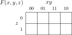
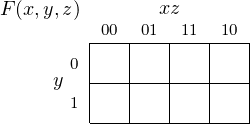
Next we consider a three-variable Karnaugh map. Table 4.1 (page 179) lists all the minterms for three
variables, x, y, and z, numbered from 0 – 7. A total of eight cells are needed, so we will draw it four cells
wide and two high. Our Karnaugh map will be drawn with y and z on the horizontal axis, and x on
the vertical. Figure 4.10 shows how the three-variable minterms map onto a Karnaugh map.
Notice the order of the bit patterns along the top of the three-variable Karnaugh map, which is chosen
such that only one variable changes value between any two adjacent cells (the adjacency property). It is the
same as a two-variable Gray code (see Table 3.7, page 156). That is, the order of the columns is such that
the yz values follow the Gray code.
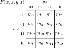
A four-variable Karnaugh map is shown in Figure 4.11. The y and z variables are on the horizontal axis,
w and x on the vertical. From this four-variable Karnaugh map we see that the order of the rows is
such that the wx values also follow the Gray code, again to implement the adjacency property.
Other axis labeling schemes also work. The only requirement is that entries in adjacent cells differ by
only one bit (which is a property of the Gray code). See Exercises 4-9 and 4-10.
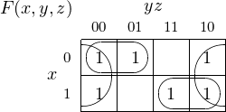
Example 4-b ______________________________________________________________________________________________________
Find a minimal sum of products expression for the function
Solution:
First we draw the Karnaugh map:
Several groupings are possible. Keep in mind that groupings can wrap around. We will work with
which yields a minimal sum of products:
__________________________________________________________________________________□
We may wish to implement a function as a product of sums instead of a sum of products. From
DeMorgan’s Law, we know that the complement of an expression exchanges all ANDs and ORs, and
complements each of the literals. The zeros in a Karnaugh map represent the complement of the expression.
So if we
- place a 0 in each cell of the Karnaugh map corresponding to a missing minterm in the expression,
- find groupings of the cells with 0s in them,
- write a sum of products expression represented by the grouping of 0s, and
- complement this expression,
we will have the desired expression expressed as a product of sums. Let us use the previous example to
illustrate.
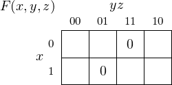
Example 4-c ______________________________________________________________________________________________________
Find a minimal product of sums for the function (repeat of Example 4-b).
Solution:
Using the Karnaugh map zeros,
we obtain the complement of our desired function,
and from DeMorgan’s Law:
__________________________________________________________________________________□
We now work an example with four variables.
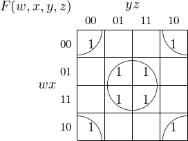
Example 4-d ______________________________________________________________________________________________________
Find a minimal sum of products expression for the function
Solution:
Using the groupings on the Karnaugh map,
we obtain a minimal sum of products,
Not only have we greatly reduced the number of AND and OR gates, we see that the two variables w and y
are not needed. By the way, you have probably encountered a circuit that implements this function. A light
controlled by two switches typically does this.
__________________________________________________________________________________□
As you probably expect by now a Karnaugh map also works when a function is specified as a product of
sums. The differences are:
- maxterms are numbered 0 for uncomplemented variables and 1 for complemented, and
- a 0 is placed in each cell of the Karnaugh map that corresponds to a maxterm.
To see how this works let us first compare the Karnaugh maps for two functions,
 | (4.32) |
 | (4.33) |
F1 is a sum of products with only one minterm, and F2 is a product of sums with only one
maxterm. Figure 4.12(a) shows how the minterm appears on a Karnaugh map, and Figure
4.12(b) shows the maxterm.
Figure 4.13 shows how three-variable maxterms map onto a Karnaugh map. As with minterms, x is on
the vertical axis, y and z on the horizontal. To use the Karnaugh map for maxterms, place a 0 is in each cell
corresponding to a maxterm.
A four-variable Karnaugh map of maxterms is shown in Figure 4.14. The w and x variables are on the
vertical axis, y and z on the horizontal.
Example 4-e ______________________________________________________________________________________________________
Find a minimal product of sums for the function
Solution:
This expression includes maxterms 0, 1, 3, 4, and 7. These appear in a Karnaugh map:
Next we encircle the largest adjacent blocks, where the number of cells in each block is a power of two. Notice
that maxterm M0 appears in two groups.
From this Karnaugh map it is very easy to write the function as a minimal product of sums:
__________________________________________________________________________________□
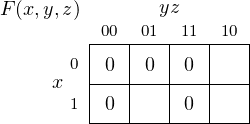
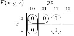
There are situations where some minterms (or maxterms) are irrelevant in a function. This might occur,
say, if certain input conditions are impossible in the design. As an example, assume that you have an
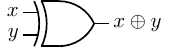
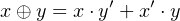
application where the exclusive or (XOR) operation is required. The symbol for the operation and its truth
table are shown in Figure 4.15.
The minterms required to implement this operation are:
This is the simplest form of the XOR operation. It requires two AND gates, two NOT gates, and an OR gate
for realization.
But let us say that we have the additional information that the two inputs, x and y can never be 1 at the
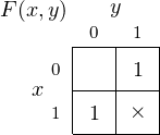
same time. Then we can draw a Karnaugh map with an “×” for the minterm that cannot exist as shown in
Figure 4.16. The “×” represents a “don’t care” cell — we don’t care whether this cell is grouped with other
cells or not.
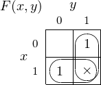
Since the cell that represents the minterm x ⋅ y is a “don’t care”, we can include it in our minimization
groupings, leading to the two groupings shown in Figure 4.17.
We easily recognize this Karnaugh map as being realizable with a single OR gate, which saves one OR
gate and an AND gate.
4.4 Crash Course in Electronics
Although it is not necessary to be an electrical engineer in order to understand how logic gates work, some
basic concepts will help. This section provides a very brief overview of the fundamental concepts of electronic
circuits. We begin with two definitions.
-
Current
- is the movement of electrical charge. Electrical charge is measured in coulombs. A flow of
one coulomb per second is defined as one ampere, often abbreviated as one amp. Current only
flows in a closed path through an electrical circuit.
-
Voltage
- is a difference in electrical potential between two points in an electrical circuit. One volt
is defined as the potential difference between two points on a conductor when one ampere of
current flowing through the conductor dissipates one watt of power.
The electronic circuits that make up a computer are constructed from:
- A power source that provides the electrical power.
- Passive elements that control current flow and voltage levels.
- Active elements that switch between various combinations of the power source, passive elements,
and other active elements.
We will look at how each of these three categories of electronic components behaves.
4.4.1 Power Supplies and Batteries
The electrical power is supplied to our homes, schools, and businesses in the form of alternating current
(AC). A plot of the magnitude of the voltage versus time shows a sinusoidal wave shape. Computer circuits
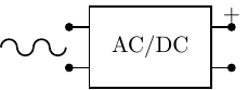
use direct current (DC) power, which does not vary over time. A power supply is used to convert AC power
to DC as shown in Figure 4.18.
As you probably know, batteries also provide DC power.
Computer circuits use DC power. They distinguish between two different voltage levels to provide logical
0 and 1. For example, logical 0 may be represented by 0.0 volts and logical 1 by +2.5 volts. Or the reverse
may be used — +2.5 volts as logical 0 and 0.0 volts as logical 1. The only requirement is that the hardware
design be consistent. Fortunately, programmers do not need to be concerned about the actual voltages
used.
Electrical engineers typically think of the AC characteristics of a circuit in terms of an ongoing sinusoidal
voltage. Although DC power is used, computer circuits are constantly switching between the two voltage
levels. Computer hardware engineers need to consider circuit element time characteristics when the voltage is
suddenly switched from one level to another. It is this transient behavior that will be described in the
following sections.
4.4.2 Resistors, Capacitors, and Inductors
All electrical circuits have resistance, capacitance, and inductance.
- Resistance dissipates power. The electric energy is transformed into heat.
- Capacitance stores energy in an electric field. Voltage across a capacitance cannot change
instantaneously.
- Inductance stores energy in a magnetic field. Current through an inductance cannot change
instantaneously.
All three of these electro-magnetic properties are distributed throughout any electronic circuit. In computer
circuits they tend to limit the speed at which the circuit can operate and to consume power, collectively
known as impedance. Analyzing their effects can be quite complicated and is beyond the scope
of this book. Instead, to get a feel for the effects of each of these properties, we will consider
the electronic devices that are used to add one of these properties to a specific location in a
circuit; namely, resistors, capacitors, and inductors. Each of these circuit devices has a different
relationship between the voltage difference across the device and the current flowing through
it.
A resistor irreversibly transforms electrical energy into heat. It does not store energy. The relationship
between voltage and current for a resistor is given by the equation
 | (4.34) |
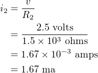
where v is the voltage difference across the resistor at time t, i is the current flowing through it at
time t, and R is the value of the resistor. Resistor values are specified in ohms. The circuit
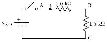
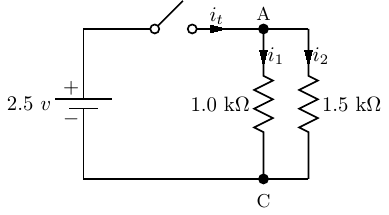
shown in Figure 4.19 shows two resistors connected in series through a switch to a battery.
The battery supplies 2.5 volts. The Greek letter Ω is used to indicate ohms, and kΩ indicates 103 ohms.
Since current can only flow in a closed path, none flows until the switch is closed.
Both resistors are in the same path, so when the switch is closed the same current flows through each of
them. The resistors are said to be connected in series. The total resistance in the path is their
sum:
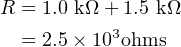 | (4.35) |
The amount of current can be determined from the application of Equation 4.34. Solving for
i,
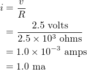 | (4.36) |
where “ma” means “milliamps.”
We can now use Equation 4.34 to determine the voltage difference between points A and
B.
 | (4.37) |
Similarly, the voltage difference between points B and C is
 | (4.38) |
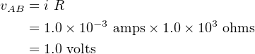
Figure 4.20 shows the same two resistors connected in parallel.
In this case, the voltage across the two resistors is the same: 2.5 volts when the switch is closed. The
current in each one depends upon its resistance. Thus,
 | (4.39) |
and
 | (4.40) |
The total current, it, supplied by the battery when the switch is closed is divided at point A to supply both
the resistors. It must equal the sum of the two currents through the resistors,
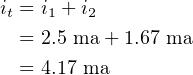 | (4.41) |
A capacitor stores energy in the form of an electric field. It reacts slowly to voltage changes, requiring
time for the electric field to build. The voltage across a capacitor changes with time according to the
equation
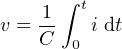 | (4.42) |
where C is the value of the capacitor in farads.
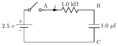
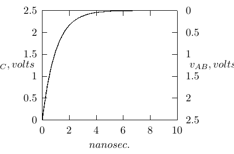
Figure 4.21 shows a 1.0 microfarad capacitor being charged through a 1.0 kilohm resistor.
This circuit is a rough approximation of the output of one transistor connected to the input of another.
(See Section 4.4.3.) The output of the first transistor has resistance, and the input to the second transistor
has capacitance. The switching behavior of the second transistor depends upon the voltage across the
(equivalent) capacitor, vBC.
Assuming the voltage across the capacitor, vBC, is 0.0 volts when the switch is first closed, current flows
through the resistor and capacitor. The voltage across the resistor plus the voltage across the capacitor must
be equal to the voltage available from the battery. That is,
 | (4.43) |
If we assume that the voltage across the capacitor, vBC, is 0.0 volts when the switch is first closed, the full
voltage of the battery, 2.5 volts, will appear across the resistor. Thus, the initial current flow in the circuit
will be
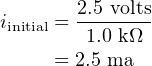 | (4.44) |
As the voltage across the capacitor increases, according to Equation 4.42, the voltage across the resistor,
vAB, decreases. This results in an exponentially decreasing build up of voltage across the capacitor. When it
finally equals the voltage of the battery, the voltage across the resistor is 0.0 volts and current flow in the
circuit becomes zero. The rate of the exponential decrease is given by the product RC, called the time
constant.
Using the values of R and C in Figure 4.21 we get
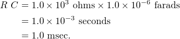 | (4.45) |
Thus, assuming the capacitor in Figure 4.21 has 0.0 volts across it when the switch is closed, the voltage
that develops over time is given by
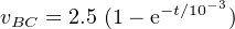 | (4.46) |
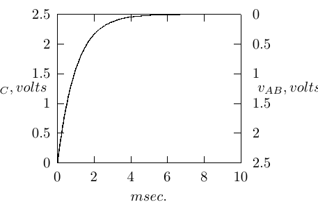
This is shown in Figure 4.22.
At the time t = 1.0 millisecond (one time constant), the voltage across the capacitor is
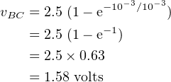 | (4.47) |
After 6 time constants of time have passed, the voltage across the capacitor has reached
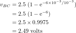 | (4.48) |
At this time the voltage across the resistor is essentially 0.0 volts and current flow is very low.
Inductors are not used in logic circuits. In the typical PC, they are found as part of the CPU power
supply circuitry. If you have access to the inside of a PC, you can probably see a small (∼1 cm. in diameter)
donut-shaped device with wire wrapped around it on the motherboard near the CPU. This is an inductor
used to smooth the power supplied to the CPU.
An inductor stores energy in the form of a magnetic field. It reacts slowly to current changes, requiring
time for the magnetic field to build. The relationship between voltage at time t across an inductor and
current flow through it is given by the equation
 | (4.49) |
where L is the value of the inductor in henrys.
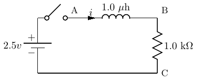
Figure 4.23 shows an inductor connected in series with a resistor.
When the switch is open no current flows through this circuit. Upon closing the switch, the
inductor initially impedes the flow of current, taking time for a magnetic field to be built up in the
inductor.
At this initial point no current is flowing through the resistor, so the voltage across it, vBC, is 0.0 volts.
The full voltage of the battery, 2.5 volts, appears across the inductor, vAB. As current begins to flow through
the inductor the voltage across the resistor, vBC, grows. This results in an exponentially decreasing voltage
across the inductor. When it finally reaches 0.0 volts, the voltage across the resistor is 2.5 volts and current
flow in the circuit is 2.5 ma.
The rate of the exponential voltage decrease is given by the time constant L∕R. Using the values of R
and L in Figure 4.23 we get
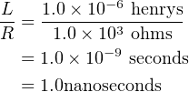 | (4.50) |
When the switch is closed, the voltage that develops across the inductor over time is given by
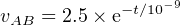 | (4.51) |
This is shown in Figure 4.24.
Note that after about 6 nanoseconds (6 time constants) the voltage across the inductor is essentially
equal to 0.0 volts. At this time the full voltage of the battery is across the resistor and a steady current of
2.5 ma flows.
This circuit in Figure 4.23 illustrates how inductors are used in a CPU power supply. The battery in this
circuit represents the computer power supply, and the resistor represents the load provided by the CPU. The
voltage produced by a power supply includes noise, which consists of small, high-frequency fluctuations
added to the DC level. As can be seen in Figure 4.24, the voltage supplied to the CPU, vBC, changes little
over short periods of time.
4.4.3 CMOS Transistors
The general idea is to use two different voltages to represent 1 and 0. For example, we might use a
high voltage, say +2.5 volts, to represent 1 and a low voltage, say 0.0 volts, to represent 0.
Logic circuits are constructed from components that can switch between these the high and low
voltages.
The basic switching device in today’s computer logic circuits is the metal-oxide-semiconductor field-effect
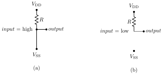
transistor (MOSFET). Figure 4.25 shows a NOT gate implemented with a single MOSFET.
The MOSFET in this circuit is an n-type. You can think of it as a three-terminal device. The input
terminal is called the gate. The terminal connected to the output is the drain, and the terminal
connected to V SS is the source. In this circuit the drain is connected to positive (high) voltage of a
DC power supply, V DD, through a resistor, R. The source is connected to the zero voltage,
V SS.
When the input voltage to the transistor is high, the gate acquires an electrical charge, thus turning the
transistor on. The path between the drain and the source of the transistor essentially become a closed
switch. This causes the output to be at the low voltage. The transistor acts as a pull down
device.
The resulting circuit is equivalent to Figure 4.26(a).
In this circuit current flows from V DD to V SS through the resistor R. The output is connected to V SS,
that is, 0.0 volts. The current flow through the resistor and transistor is
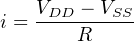 | (4.52) |
The problem with this current flow is that it uses power just to keep the output low.
If the input is switched to the low voltage, the transistor turns off, resulting in the equivalent circuit
shown in Figure 4.26(b). The output is typically connected to another transistor’s input (its gate), which
draws essentially no current, except during the time it is switching from one state to the other. In the steady
state condition the output connection does not draw current. Since no current flows through the resistor, R,
there is no voltage change across it. So the output connection will be at V DD volts, the high voltage. The
resistor is acting as the pull up device.
These two states can be expressed in the truth table
input | output |
|
|
low | high |
high | low |
|
which is the logic required of a NOT gate.
There is another problem with this hardware design. Although the gate of a MOSFET transistor
draws essentially no current in order to remain in either an on or off state, current is required to
cause it to change state. The gate of the transistor that is connected to the output must be
charged. The gate behaves like a capacitor during the switching time. This charging requires
a flow of current over a period of time. The problem here is that the resistor, R, reduces the
amount of current that can flow, thus taking larger to charge the transistor gate. (See Section
4.4.2.)
From Equation 4.52, the larger the resistor, the lower the current flow. So we have a dilemma — the
resistor should be large to reduce power consumption, but it should be small to increase switching
speed.
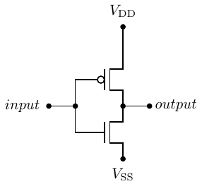
This problem is solved with Complementary Metal Oxide Semiconductor (CMOS) technology. This
technology packages a p-type MOSFET together with each n-type. The p-type works in the opposite way —
a high value on the gate turns it off, and a low value turns it on. The circuit in Figure 4.27 shows a NOT
gate using a p-type MOSFET as the pull up device.
Figure 4.28(a) shows the equivalent circuit with a high voltage input. The pull up transistor (a p-type) is
off, and the pull down transistor (an n-type) is on. This results in the output being pulled down to the low
voltage.
In Figure 4.28(b) a low voltage input turns the pull up transistor on and the pull down transistor off. The
result is the output is pulled up to the high voltage.
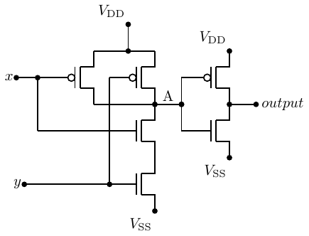
Figure 4.29 shows an AND gate implemented with CMOS transistors.
(See Exercise 4-12.) Notice that the signal at point A is NOT(x AND y). The circuit from point A to the
output is a NOT gate. It requires two fewer transistors than the AND operation. We will examine the
implications of this result in Section 4.5.
4.5 NAND and NOR Gates
The discussion of transistor circuits in Section 4.4.3 illustrates a common characteristic. Because of the
inherent way that transistors work, most circuits invert the signal. That is, a high voltage at the input
produces a low voltage at the output and vice versa. As a result, an AND gate typically requires a NOT gate
at the output in order to achieve a true AND operation.
We saw in that discussion that it takes fewer transistors to produce AND NOT than a pure AND. The
combination is so common, it has been given the name NAND gate. And, of course, the same is true for OR
gates, giving us a NOR gate.
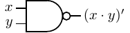
- NAND — a binary operator; the result is 0 if and only if both operands are 1; otherwise the result is 1.
We will use (x ⋅ y)′ to designate the NAND operation. It is also common to use the ’↑’ symbol or
simply “NAND”. The hardware symbol for the NAND gate is shown in Figure 4.30. The
inputs are x and y. The resulting output, (x ⋅ y)′, is shown in the truth table in this figure.
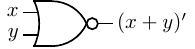
- NOR — a binary operator; the result is 0 if at least one of the two operands is 1; otherwise the result
is 1. We will use (x + y)′ to designate the NOR operation. It is also common to use the ’↓’ symbol or
simply “NOR”. The hardware symbol for the NOR gate is shown in Figure 4.31. The inputs
are x and y. The resulting output, (x + y)′, is shown in the truth table in this figure.
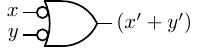
The small circle at the output of the NAND and NOR gates signifies “NOT”, just as with the NOT gate
(see Figure 4.3). Although we have explicitly shown NOT gates when inputs to gates are complemented, it is
common to simply use these small circles at the input. For example, Figure 4.32 shows an OR gate with
both inputs complemented.
As the truth table in this figure shows, this is an alternate way to draw a NAND gate. See Exercise 4-14
for an alternate way to draw a NOR gate.
One of the interesting properties about NAND gates is that it is possible to build AND, OR, and NOT
gates from them. That is, the NAND gate is sufficient to implement any Boolean function. In this sense, it
can be thought of as a universal gate.
First, we construct a NOT gate. To do this, simply connect the signal to both inputs of a NAND gate, as
shown in Figure 4.33.
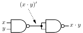
Next, we can use DeMorgan’s Law (Equation 4.17) to derive an AND gate.
 | (4.53) |
So we need two NAND gates connected as shown in Figure 4.34.
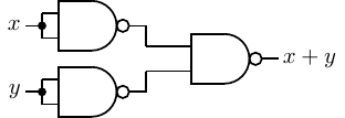
Again, using DeMorgan’s Law (Equation 4.16)
 | (4.54) |
we use three NAND gates connected as shown in Figure 4.35 to create an OR gate.
It may seem like we are creating more complexity in order to build circuits from NAND gates. But
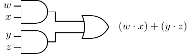
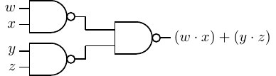
consider the function
 | (4.55) |
Without knowing how logic gates are constructed, it would be reasonable to implement this function with
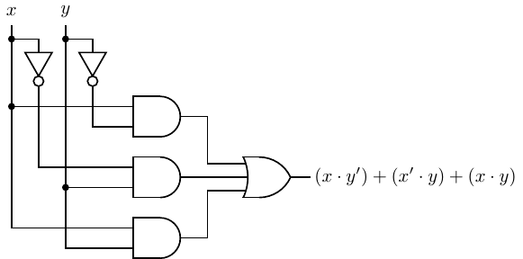
the circuit shown in Figure 4.36.
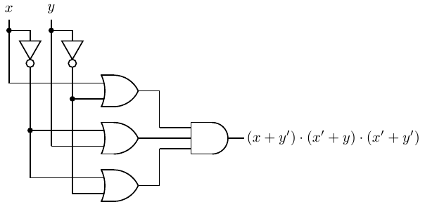
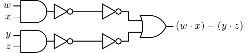
Using the involution property (Equation 4.15) it is clear that the circuit in Figure 4.37 is equivalent to
the one in Figure 4.36.
Next, comparing the AND-gate/NOT-gate combination with Figure 4.30, we see that each is simply a
NAND gate. Similarly, comparing the NOT-gates/OR-gate combination with Figure 4.32, it is also a NAND
gate. Thus we can also implement the function in Equation 4.55 with three NAND gates as shown in Figure
4.38.
From simply viewing the circuit diagrams, it may seem that we have not gained anything in this circuit
transformation. But we saw in Section 4.4.3 that a NAND gate requires fewer transistors than an AND gate
or OR gate due to the signal inversion properties of transistors. Thus, the NAND gate implementation is a
less expensive and faster implementation.
The conversion from an AND/OR/NOT gate design to one that uses only NAND gates is
straightforward:
- Express the function as a minimal SoP.
- Convert the products (AND terms) and the final sum (OR) to NANDs.
- Add a NAND gate for any product with only a single literal.
As with software, hardware design is an iterative process. Since there usually is not a unique solution, you often
need to develop several designs and analyze each one within the context of the available hardware.
The example above shows that two solutions that look the same on paper may be dissimilar in
hardware.
In Chapter 6 we will see how these concepts can be used to construct the heart of a computer — the
CPU.
4.6 Exercises
-
4-1
-
(§4.1) Prove the identity property expressed by Equations 4.3 and 4.4.
-
4-2
-
(§4.1) Prove the commutative property expressed by Equations 4.5 and 4.6.
-
4-3
-
(§4.1) Prove the null property expressed by Equations 4.7 and 4.8.
-
4-4
-
(§4.1) Prove the complement property expressed by Equations 4.9 and 4.10.
-
4-5
-
(§4.1) Prove the idempotent property expressed by Equations 4.11 and 4.12.
-
4-6
-
(§4.1) Prove the distributive property expressed by Equations 4.13 and 4.14.
-
4-7
-
(§4.1) Prove the involution property expressed by Equation 4.15.
-
4-8
-
(§4.2) Show that Equations 4.18 and 4.19 represent the same function. This shows that the sum
of minterms and product of maxterms are complementary.
-
4-9
-
(§4.3.2) Show where each minterm is located with this Karnaugh map axis labeling using the notation
of Figure 4.10.
-
4-10
-
(§4.3.2) Show where each minterm is located with this Karnaugh map axis labeling using the notation
of Figure 4.10.
-
4-11
-
(§4.3.2) Design a logic function that detects the prime single-digit numbers. Assume that the numbers
are coded in 4-bit BCD (see Section 3.6.1, page 145). The function is 1 for each prime
number.
-
4-12
-
(§4.4.3) Using drawings similar to those in Figure 4.28, verify that the logic circuit in Figure 4.29 is an
AND gate.
-
4-13
-
(§4.5) Show that the gate in Figure 4.32 is a NAND gate.
-
4-14
-
(§4.5) Give an alternate way to draw a NOR gate, similar to the alternate NAND gate in Figure
4.32.
-
4-15
-
(§4.5) Design a circuit using NAND gates that detects the “below” condition for two 2-bit values. That
is, given two 2-bit variables x and y, F(x,y) = 1 when the unsigned integer value of x is less than the
unsigned integer value of y.
-
a)
-
Give a truth table for the output of the circuit, F.
-
b)
-
Find a minimal sum of products for F.
-
c)
-
Implement F using NAND gates.