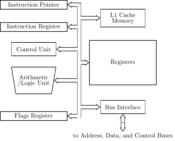
Figure 6.1: CPU block diagram. The CPU communicates with the Memory and I/O subsystems via
the Address, Data, and Control buses. See Figure 1.1 (page 9).
In this chapter we move on to consider a programmer’s view of the Central Processing Unit (CPU) and how it interacts with memory. X86-64 CPUs can be used with either a 32-bit or a 64-bit operating system. The CPU features available to the programmer depend on the operating mode of the CPU. The modes of interest to the applications programmer are summarized in Table 6.1. With a 32-bit operating system, the CPU behaves essentially the same as an x86-32 CPU.
| Mode | Submode | Operating | Default | Default |
| System | Address (bits) | int (bits) | ||
| 64-bit | 64 | |||
| IA-32e or | 64-bit | 32 | 32 | |
| Long | Compatibility | 16 | 16 | |
| 32 | 32 | |||
| Protected | ||||
| Legacy | Virtual-8086 | 32-bit | 16 | 16 |
| Real | 16-bit | |||
In this book we describe the view of the CPU when running a 64-bit operating system. Intel manuals call this the IA-32e mode and the AMD manuals call it the long mode. The CPU can run in one of two sub-modes under a 64-bit operating system. Both manuals use the same terminology for the two sub-modes.
The two modes cannot be mixed in the same program.
The discussion in this chapter focuses on the 64-bit mode. We will also point out the differences of the compatibility mode, which we will refer to as the 32-bit mode.
An overall block diagram of a typical CPU is shown in Figure 6.1.
The subsystems are connected together through internal buses. Keep in mind that this is a highly simplified diagram. Actual CPUs are much more complicated, but the general concepts discussed in this chapter apply to all of them.
We will now describe briefly each of the subsystems in Figure 6.1. The descriptions provided here are generic and apply to most CPUs. Components that are of particular interest to a programmer are described within the context of the x86 ISA later in this chapter.
We will now look at how the logic circuits discussed in Chapter 4 can be used to implement some of these subsystems.
A portion of the memory in the CPU is organized into registers. Machine instructions access CPU registers by their addresses, just as memory contents are accessed. Of course, the register addresses are not placed on the address bus since the registers are in the CPU. The difference from a programmer’s point of view is that the assembler has predefined names for the registers, whereas the programmer creates symbolic names for memory addresses. Thus in each program that you write in assembly language:
The x86-64 architecture registers are shown in Table 6.2.
| Basic Programming Registers
| |||
| 16 | 64-bit | General purpose (GPRs) | |
| 1 | 64-bit | Flags | |
| 1 | 64-bit | Instruction pointer | |
| 6 | 16-bit | Segment | |
| Floating Point Registers
| |||
| 8 | 80-bit | Floating point data | |
| 1 | 16-bit | Control | |
| 1 | 16-bit | Status | |
| 1 | 16-bit | Tag | |
| 1 | 11-bit | Opcode | |
| 1 | 64-bit | FPU Instruction Pointer | |
| 1 | 64-bit | FPU Data Pointer | |
| MMX Registers
| |||
| 8 | 64-bit | MMX | |
| XMM Registers
| |||
| 16 | 128-bit | XMM | |
| 1 | 32-bit | MXCSR | |
| Model-Specific Registers (MSRs)
| |||
| These vary depending on the specific
| |||
| hardware implementation. They are only
| |||
| accessible to the operating system.
| |||
Each bit in each register is numbered from right to left, beginning with zero. So the right-most bit is number 0, the next one to the left number 1, etc. Since there are 64 bits in each register, the left-most bit is number 63.
The general purpose registers can be accessed in the following ways:
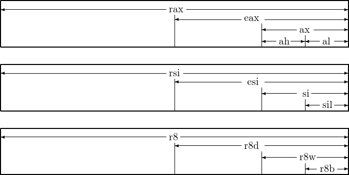
The assembler uses a different name for each group of bits in a register. The assembler names for the groups of the bits are given in Table 6.3. In 64-bit mode, writing to an 8-bit or 16-bit portion of a register does not affect the other 56 or 48 bits in the register. However, when writing to the low-order 32 bits, the high-order 32 bits are set to zero.
| bits 63-0 | bits 31-0 | bits 15-0 | bits 15-8 | bits 7-0 |
| rax | eax | ax | ah | al |
| rbx | ebx | bx | bh | bl |
| rcx | ecx | cx | ch | cl |
| rdx | edx | dx | dh | dl |
| rsi | esi | si |
| sil |
| rdi | edi | di |
| dil |
| rbp | ebp | bp |
| bpl |
| rsp | esp | sp |
| spl |
| r8 | r8d | r8w |
| r8b |
| r9 | r9d | r9w |
| r9b |
| r10 | r10d | r10w |
| r10b |
| r11 | r11d | r11w |
| r11b |
| r12 | r12d | r12w |
| r12b |
| r13 | r13d | r13w |
| r13b |
| r14 | r14d | r14w |
| r14b |
| r15 | r15d | r15w |
| r15b |
A pictorial representation of the naming of each portion of the general-purpose registers is shown in Figure 6.2.
The 8-bit register portions ah, bh, ch, and dh are a holdover from the Intel® 8086/8088 architecture. It had four 16-bit registers, ax, bx, cx, and dx. The low-order bytes were named al, bl, cl, and dl and the high-order bytes named ah, bh, ch, and dh. Access to these registers has been maintained in 32-bit mode for backward compatibility but is limited in 64-bit mode. Access to the 8-bit low-order portions of the rsi, rdi, rsp, and rbp registers was added along with the move to 64 bits in the x86-64 architecture but cannot be used in the same instruction with the 8-bit register portions of the xh registers.
Although these are called “general purpose,” the descriptions in Table 6.4 show that some of them have some special significance, depending upon how they are used. (Some of the descriptions may not make sense to you at this point.)
| Register | Special usage | Called function preserves contents |
| rax | 1st function return value. | No |
| rbx | Optional base pointer. | Yes |
| rcx | Pass 4th argument to function. | No |
| rdx | Pass 3rd argument to function; 2nd function return value. | No |
| rsp | Stack pointer. | Yes |
| rbp | Optional frame pointer. | Yes |
| rdi | Pass 1st argument to function. | No |
| rsi | Pass 2nd argument to function. | No |
| r8 | Pass 5th argument to function. | No |
| r9 | Pass 6th argument to function. | No |
| r10 | Pass function’s static chain pointer. | No |
| r11 |
| No |
| r12 |
| Yes |
| r13 |
| Yes |
| r14 |
| Yes |
| r15 |
| Yes |
In this book, we will use the rax, rdx, rdi, esi, and r8 – r15 registers for general-purpose storage. They will be used just like variables in a high-level language. Usage of the rsp and rbp registers follows a very strict discipline. You should not use either of them for your assembly language programs until you understand how to use them.
The instruction pointer register, rip1 , always points to the next instruction to be executed. As explained in Section 6.4 (page 479), every time an instruction is fetched, the rip register is automatically incremented by the control unit to contain the address of the next instruction. Thus, the rip register is never directly accessed by the programmer. On the other hand, every instruction that is executed affects the contents of the rip register. Thus, the rip register is not a general-purpose register, but it guides the flow of the entire program.
Most arithmetic and logical operations affect the condition codes in the rflags register. The bits that are affected are shown in Figure 6.3.

The names of the condition codes are:
| OF | Overflow Flag |
| SF | Sign Flag |
| ZF | Zero Flag |
| AF | Auxiliary carry or Adjust Flag |
| PF | Parity Flag |
| CF | Carry Flag |
The OF, SF, ZF, and CF are described at appropriate places in this book. See [3] and [14] for descriptions of the other flags.
Two other registers are very important in a program. The rsp register is used as a stack pointer, as will be discussed in Section 8.2 (page 551). The rbp register is typically used as a base pointer; it will be discussed in Section 8.4 (page 574).
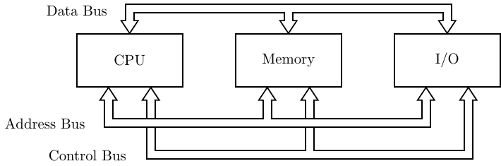
The connections between the CPU and Memory are shown in Figure 6.4. This figure also includes the I/O (input and output) subsystem. The I/O system will be discussed in subsequent chapters. The control unit is connected to memory by three buses:
As an example of how data can be stored in memory, let us imagine that we have some data in one of the CPU registers. Storing this data in memory is effected by setting the states of a group of bits in memory to match those in the CPU register. The control unit can be programmed to do this by
For example, if the eight bits in memory at address 0x7fffd9a43cef are in the state:
the al register in the CPU is in the state:
and the control unit is programmed to store this value at location 0x7fffd9a43cef, the control unit then
Then the bits at memory location 0x7fffd9a43cef will be changed to the state:
Important. When the state of any bit in memory or in a register is changed any previous states are lost forever. There is no way to “undo” this state change or to determine how the bit got in its current state.
You may be wondering how the CPU is programmed. It contains a special register — the instruction register — whose bit pattern determines what the CPU will do. Once that action has been completed, the bit pattern in the instruction register can be changed, and the CPU will perform the operation specified by this next bit pattern.
Since instructions are simply bit patterns, they can be stored in memory. The instruction pointer register always has the memory address of (points to) the next instruction to be executed. In order for the control unit to execute this instruction, it is copied into the instruction register.
The situation is as follows:
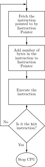
Steps 3, 4, and 5 are called an instruction fetch. Notice that steps 3 – 8 constitute a cycle, the instruction execution cycle. It is shown graphically in Figure 6.5.
This raises a couple of questions:
The source file is written in a programming language, e.g., C++. This is very similar to creating a file with a word processor. The main differences are that an editor is much simpler than a word processor, and the contents of the source file are written in the programming language instead of, say, English.
The compiler translates the programming language in a source file into the bit patterns that can be used by a CPU (machine language). The source file contents remains unchanged.
Most programs are made up of several object files. For example, a GNU/Linux installation includes many object files that contain the machine instructions to perform common tasks. These are programs that have already been written and compiled. Related tasks are commonly grouped together into a single file called a library.
Whenever possible, you should use the short programs in these libraries to perform the computations your program needs rather that write it yourself. The linker program will merge the machine code from these several object files into one file.
You may have used an integrated development environment (IDE), e.g., Microsoft®Visual Studio®, Eclipse™, which combines all of these three programs into one package where each of the intermediate steps is performed automatically. You use the editor program to create the source file and then give the run command to the IDE. The IDE will compile the program in your source files, link the resulting object files with the necessary libraries, load the resulting executable file into memory, then start your program. In general, the intermediate object files resulting from the compilation of each source file are automatically deleted from the disk.
In this book we will explicitly perform each of these steps separately so we can learn the role of each program — editor, assembler, linker — used in preparing the application program.
We will use the program in Listing 6.1 to illustrate the use of gdb to view the contents of the CPU registers. I have used the register storage class modifier to request that the compiler use a CPU register for the int* ptr variable. The register modifier is “advisory” only. See Exercise 6-3 for an example when the compiler may not be able to honor our request.
We introduced some gdb commands in Chapter 2. Here are some additional ones that will be used in this section:
Here is a screen shot of how I compiled the program then used gdb to control the execution of the program and observe the register contents. My typing is boldface and the session is annotated in italics. Note that you will probably see different addresses if you replicate this example on your own (Exercise 6-1).
bob$ gcc -g -O0 -Wall -fno-asynchronous-unwind-tables \
> -fno-stack-protector -o gdbExample1 gdbExample1.c
The “-g” option is required. It tells the compiler to include debugger information in the executable program.
 n", wye);
The li command lists ten lines of source code. The display is centered around the current line. Since I have not started execution of this program, the display is centered around the beginning of main. The display ends with the (gdb) prompt. Pushing the return key repeats the previous command, and li is smart enough to display the next ten lines.
I set a breakpoint at line 19 then run the program. When line 19 is reached, the program is paused before the statement is executed, and control returns to gdb.
I use the print command to view the value assigned to the ex variable and learn its memory address.
The help command will provide very brief instructions on using a command. We want to display values stored in specific memory locations in various formats, and the help command provides a reminder of how to use the command.
I verify that the value assigned to the ex variable is stored at location 0x7fffffffe044.
I examine the same integer in hexadecimal format.
Next, I examine all four bytes of the word, one byte at a time. In this display,
In other words, the byte-wise display appears to be backwards. This is due to the values being stored in the little endian storage scheme as explained on page 46 in Chapter 2.
I also examine all four bytes of the word, two bytes at a time. In this display,
This shows how gdb displays these four bytes as though they represent two 16-bit ints stored in little endian format. (You can now see why I entered such a strange integer in this demonstration run.)
Look carefully at the ptr variable. It is located at address 0x7fffffffe048 and it contains another address, 0x7fffffffe044, that is, the address of the variable ex. It is important that you learn to distinguish between a memory address and the value that is stored there, which can be another memory address. Perhaps a good way to think about this is a group of numbered mailboxes, each containing a single piece of paper that you can write a single number on. You could write a number that represents a “data” value on the paper. Or you can write the address of a mailbox on the paper. One of the jobs of a programmer is to write the program such that it interprets the number appropriately — either a data value or an address.
The compiler has honored our request and allocated a register for the wye variable. Registers are located in the CPU and do not have memory addresses, so gdb cannot print the address. We will need to use the i r command to view the register contents.
The i r command displays the current contents of the CPU registers. The first column is the name of the register. The second shows the current bit pattern in the register, in hexadecimal. Notice that leading zeros are not displayed. The third column shows some the register contents in 64-bit signed decimal. The registers that always hold addresses are also shown in hexadecimal in the third column. The columns are often not aligned due to the tabbing of the display.
We see that the value in the ebx general purpose register is the same as that stored in the wye variable, 0xffffffff.3 (Recall that ints are 32 bits, even in 64-bit mode.) We conclude that the compiler chose to allocate ebx as the wye variable.
Notice the value in the rip register, 0x4005a9. Refer back to where I set the breakpoint on source line 19. This shows that the program stopped at the correct memory location.
It is only coincidental that the address of the ex variable is currently stored in the rax register. If a general purpose register is not allocated as a variable within a function, it is often used to store results of intermediate computations. You will learn how to use registers this way in subsequent chapters of this book.
These two breakpoints will allow us to examine the value stored in the wye variable just before and after it is modified.
This verifies that the user’s input value is stored correctly and that the wye variable has not yet been changed.
 n", wye);
And this verifies that our (rather simple) algorithm works correctly.
We can specify which registers to display with the i r command. This verifies that the rbx register is being used as the wye variable.
And we see that the rip has incremented from 0x4005a9 to 0x4005d6. Don’t forget that the rip register always points to the next instruction to be executed.
Finally, I continue to the end of the program. Notice that gdb is still running and I have to quit the gdb program.
(§6.2, §6.5) Enter the program in Listing 6.1 and trace through the program one line at a time using gdb. Use the n command, not s or si. Keep a written record of the rip register at the beginning of each line. Hint: use the i r command. How many bytes of machine code are in each of the C statements in this program? Note that the addresses you see in the rip register may differ from the example given in this chapter.
(§6.2, §6.4) As you trace through the program in Exercise 6-1 stop on line 22:
We determined in the example above that the %rbx register is used for the variable wye. Inspect the registers.
What is the address of the first instruction that will be executed when you enter the n command?
How will %rbx change when this statement is executed?
(§6.5) Modify the program in Listing 6.1 so that a register is also requested for the ex variable. Were you able to convince the compiler to do this for you? Did the compiler produce any error or warning messages? Why do you think the compiler would not use a register for this variable.
(§6.2, §6.5) Use the gdb debugger to observe the contents of memory in the program from Exercise 2-31. Verify that your algorithm creates a null-terminated string without the newline character.
(§6.2, §6.5) Write a program in C that allows you to determine the endianess of your computer. Hint: use unsigned char* ptr.
(§6.2, §6.5) Modify the program in Exercise 6-5 so that you can demonstrate, using gdb, that endianess is a property of the CPU. That is, even though a 32-bit int is stored little endian in memory, it will be read into a register in the “proper” order. Hint: declare a second int that is a register variable; examine memory one byte at a time.